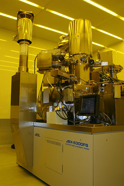
May 5, 2015 - Peabody, MA -- A state-of-the-art JEOL e-beam lithography system will soon be a new resource for quantum information science researchers that utilize the cutting-edge facilities at the University of Waterloo Quantum NanoFab in Waterloo, Ontario. The JEOL JBX-6300FS e-beam system will be used to write circuitry patterns at very high resolution and linewidths as small as 8nm. With accelerating voltage capability to 100kV, high resolution patterns can be written on substrates coated in thick resist.
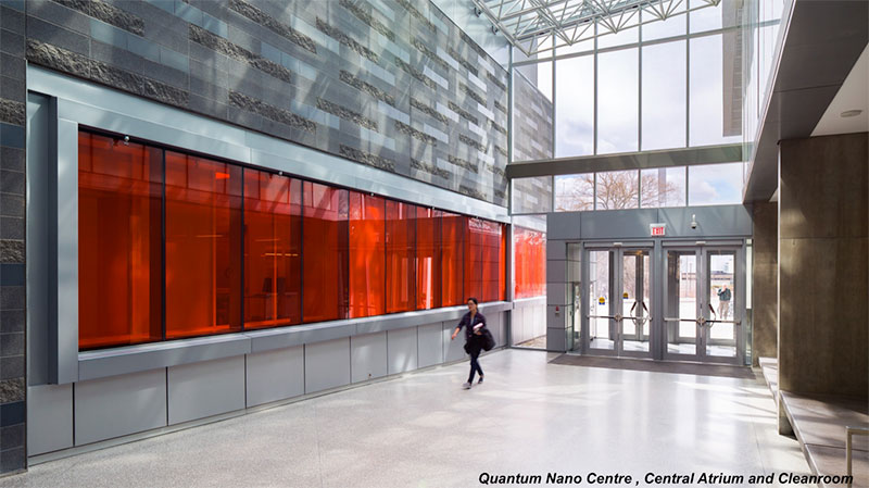
University of Waterloo Quantum Nanofab
"We're very excited to obtain this 100kV system." said Vito Logiudice, Director of Operations for the Quantum NanoFab. "This opens the lab up for certain types of research where people need to use thick resist all while pushing the limits on minimum feature size." The new system will be an integral part of the Quantum Nanofab's goal of providing the tools needed for next-generation quantum devices.
The challenge of creating ever more powerful microchips, which continue to shrink in size, demands new technologies on the scale of individual atoms, or the quantum scale. Through the work being done in the Quantum Nanofab, which serves the Institute for Quantum Computing (IQC) and the Waterloo Institute for Nanotechnology (WIN), the University of Waterloo is poised to make that leap. Researchers will be able to "corral" single electrons through the lithography patterns they will write using the JEOL JBX-6300FS.
"This new e-beam system is going to be extremely helpful in that regard. They will be able to further advance their work on gate defined quantum dots with metal gates < 20nm wide and metal-to-metal spacing of less than 40nm," Logiudice explains. The e-beam will also write both large and very fine features in the same layer on the substrate, using high resolution as well as coarse writing modes, which can be programmed into a batch process run overnight. “This will be of great benefit for the writing of superconducting Josephson junction qubits and the microwave circuits that are used to manipulate their states.” adds Nathan Nelson-Fitzpatrick, Nanofabrication Process Engineer on the Quantum NanoFab team.
JBX 6300FS Offers Flexible User Experience
Washington Nanofabrication Facility
An attractive aspect of the JBX 6300FS is the wide spectrum of user experience the system can now accommodate. The University of Waterloo is teaming up with JEOL and Cornell University’s Nanofabrication Facility to showcase the system’s dual interfaces, both a traditional GUI/Graphical User Interface and a powerful Python-based scripting language. With scripting, power users can manipulate incoming data and perform exposures based on non-periodic arrays or logarithmic dose arrays, for example. However, that same scripting power allows the creation of new GUI’s based on the comfort or training level of the user.
"The 6300FS hardware is as flexible as the software, a core strength that comes from being one of the founding EBL solutions providers in the industry that has continually provided the latest in technology for advances in research," said JEOL EBL product manager, Zane Marek. "Though the University of Waterloo continues to grow, their substrates might actually start to shrink. As research on exotic materials continues - and those substrate prices remain 'exotic' - JEOL has secured the ability to confidently load and expose them."
Marek added, "We have the best customers in the world. They work with us and their peers at other facilities to discover novel ways to load and expose the smallest of these exotic materials. We really are in this together."
Technology Hub in Waterloo
University of Waterloo Quantum Nanofab
Known as the Quantum Valley, the Waterloo Region is home to the Institute for Quantum Computing (IQC) and the Waterloo Institute for Nanotechnology (WIN) at the University of Waterloo. The Quantum NanoFab serves both institutes in its location in the 280,000 sq. ft. Mike & Ophelia Lazaridis Quantum-Nano Centre. Since its opening in September 2014, the Quantum NanoFab has been host to some 90 new users under the direction of 25 different faculty members at the university. Plans are in place to allow more users from outside the university in the near future.
The University of Waterloo boasts a unique Intellectual Property policy where IP is inventor owned. “This policy attracts entrepreneurs and researchers to the University of Waterloo,” says Loguidice. “Coupled with the largest co-op program in North America, Waterloo gives our students a definite edge for their future endeavors both in the private and public sectors."
JEOL EBL Expertise
JEOL has a long history of e-beam innovation and expertise, with more than 45 years of design, production, and support of the company's lithography tools, which include photomask writing and direct write systems. The JBX-6300FS can easily write patterns down to 8nm or less using an electron optics system that automatically adjusts a 2.1nm electron beam at 100kV accelerating voltage. It also achieves high field-stitching and overlay accuracy of 9nm or less, providing high cost performance. A unique automatic correction function developed by JEOL enables high-precision pattern writing. The JBX-6300FS can write highly precise patterns even at field corners and boundaries by the use of its powerful electron optical system that automatically corrects distortions generated by beam deflection.
The company's serves the Americas with both sales and support through its main USA office in Peabody, Massachusetts, and with offices in Canada, Mexico, and Brasil.