RALEIGH, N.C. (October 22, 2026): A team from North Carolina State University, Oak Ridge National Laboratory (ORNL) and JEOL Ltd. has 3D printed full-size tungsten tiles for the inside wall of a fusion device, finished them to tight tolerances and tested them in the DIII-D National Fusion Facility in San Diego. The tile surfaces were directly exposed to 74 plasma discharges with significant heat and particle flux, and came through intact.
The project went from invitation to installed hardware in about eight months. It came out of NC State's research partnership with DIII-D National Fusion Facility and brought together three groups with deep expertise in electron-beam powder bed fusion (EB-PBF) and tungsten additive manufacturing. For this project, JEOL's large-format EB-PBF system and engineering team in Japan made printing the tiles at full size possible, ORNL contributed fusion materials expertise and funding, and NC State led the finishing and characterization.
"When DIII-D asked if we could do this, I said yes without blinking and then figured we'd have to sort out the details," said Dr. Tim Horn, Associate Professor of mechanical and aerospace engineering and research director at the Center for Additive Manufacturing and Logistics (CAMAL) at NC State. "Our 'Think and Do' motto aside, in reality, there were major challenges to making this happen. We understood the processing science behind tungsten additive manufacturing and the physics of scaling up. What we needed was the hardware and partners who could move fast. ORNL and JEOL were exactly that."
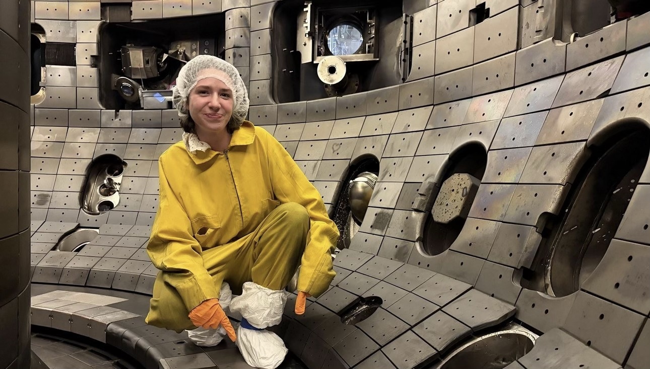
NC State nuclear engineering undergraduate Olivia Mehalick inside the DIII-D vacuum vessel during installation of the 3D-printed tungsten tiles.
Why tungsten, and why it's hard
In a fusion tokamak like DIII-D, the core plasma temperature reaches well over 100 million °C. Much of its exhaust heat lands on the divertor, a region at the bottom of the machine lined with protective tiles. In ITER and future power plants, those tiles must handle steady heat loads of 10 to 20 megawatts per square meter, more than 10,000 times the intensity of direct sunlight on a summer day, with brief bursts far higher. That means the tile material has to do several jobs at once: survive extreme heat and constant bombardment by plasma particles and high-energy neutrons, and conduct heat well enough to carry that load away.
Tungsten is considered a leading material for the job. It has the highest melting point of any metal, 3,422 °C (6,192 °F), more than twice that of steel. It is also dense: at 19.3 grams per cubic centimeter, it weighs about 2.4 times as much as steel for the same size, roughly as much as gold. For comparison, a bowling ball made of tungsten would weigh more than 100 kilograms (~225 lbs), about 14 times as much as a regulation ball.
The problem with making tungsten parts is the ductile-to-brittle transition temperature (DBTT). Below roughly 200 to 600 °C, tungsten cracks rather than bends, behaving more like glass than metal. That makes it very hard to manufacture with traditional machining or joining processes, and the high melting temperature rules out most casting and forming processes, so there is a significant amount of research effort focused on additive manufacturing, or 3D printing, approaches. However, most attempts to 3D print tungsten, nearly all using lasers as the heat source for printing, have ended up porous and riddled with cracks.
Several years ago, ORNL and NC State pioneered a different approach: electron-beam powder bed fusion (EB-PBF). An electron beam melts tungsten powder layer by layer in a vacuum chamber while the fast scanning capability of an electron beam keeps the surrounding material hot and held above 1,400 °C, well above the brittle range. The partners produced dense, crack-free tungsten this way and published the results in 2021 in the Journal of Nuclear Materials. That work helped lead to a joint ARPA-E / DOE Fusion Energy Sciences program on tungsten under ARPA-E's GAMOW initiative where Dr. Michael Kirka and Dr. Chris Ledford at ORNL led further developments on EB-PBF of tungsten.
"Tungsten is currently the material everyone wants in a fusion reactor, but it is extremely difficult to manufacture into complex shapes," Kirka said. "We were able to do this with electron-beam additive manufacturing, when most of the field thought printed tungsten would always crack. These tiles are the payoff from years of that work."
How the collaboration came together
NC State and DIII-D already work closely on the plasma physics side. Dr. Florian Laggner, an assistant professor and plasma physicist in NC State's Department of Nuclear Engineering, leads a collaboration with DIII-D's neutral beam team to develop new radio-frequency ion sources for the beams that heat the facility's plasma. His group is now assembling a 200-kilowatt prototype source at NC State.
The tile project grew out of the materials side of that relationship, where plasma physics meets advanced manufacturing. NC State joined the DIII-D program as a participating organization to enable university researchers to more rapidly advance their work using internal funds. This access, led by Laggner and Horn, is allowing them to develop and test new ways to make the materials that line the inside of fusion reactors.
In 2025, that partnership put small buttons of NC State's printed tungsten into DIII-D using the facility's Divertor Materials Evaluation System (DiMES). In tests led by NC State nuclear engineering Ph.D. student Aaliyah Zuniga, the samples saw heat fluxes near 20 megawatts per square meter, with brief peaks above 35, and showed minimal surface damage.
Those results earned an invitation. In December 2025, Dr. Jonathan Coburn of Sandia National Laboratories, who led the novel tile portion of DIII-D's 2026 Tungsten Tile Testing campaign, asked the NC State team to test a full-size printed tile.
"The AM tungsten performed quite well during Aaliyah's DiMES testing, so there was both motivation and confidence for producing a larger component for further testing," Coburn said.
The catch was scale. The DIII-D tile for this effort measures about 140 by 130 millimeters, and the largest tungsten part NC State had printed was about 50 millimeters across. It was clear that NC State's own machines could not hold such a high-temperature material at the required conditions over a build that large.
Haozhi Zhang, a postdoctoral researcher in Horn's lab who works on electron-beam printing of tungsten, looked into what it would take to print and finish a part that large, from new scan strategies to keeping a much bigger build area hot enough while it melts. "Testing an additively manufactured, full-size tungsten tile at DIII-D would be a first-of-its-kind achievement in the field," Zhang said.
Scaling up with JEOL
That is where JEOL came in. At the time, JEOL was already partnering with ORNL on additive manufacturing and placing one of its systems at the laboratory, and had recently begun developing tungsten printing independently on its own systems. And when the DIII-D invitation arrived, Horn happened to be in Japan visiting JEOL to discuss tungsten printing. It quickly became clear that JEOL's large-format EB-PBF system, the JAM-5200EBM, with its open control system, and JEOL's expertise could build the full-size tiles.
JEOL is, perhaps, best known worldwide for its scanning and transmission electron microscopes, but the company also has a long history in electron beam welding and electron beam lithography. Building a metal 3D printer around a precisely steered electron beam was a logical evolution, and the JAM-5200EBM draws on decades of JEOL's experience designing and building precision electron beam systems.
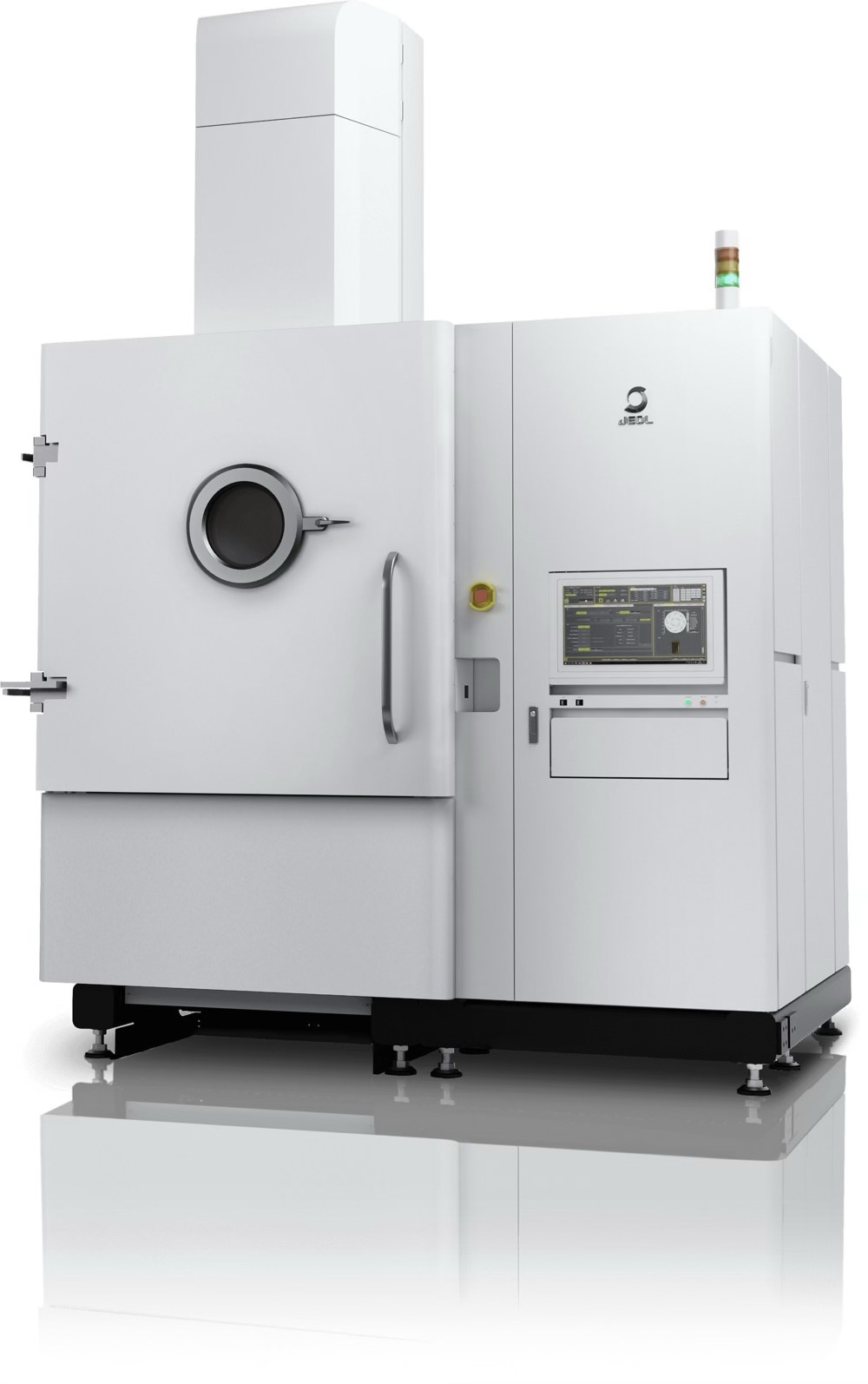
JEOL's JAM-5200EBM, the large-format electron-beam powder bed fusion system used to print the full-size tungsten tiles. Image: JEOL
In early 2026, with the DIII-D proposal accepted, Horn and Laggner brought together Zane Marek and Jonathan Buckley of JEOL USA and Michael Kirka and Christopher Ledford of ORNL. JEOL engineers Satoshi Ono and Akimine Hatsuda printed the tiles at JEOL's facility in Akishima, Japan, with Zane Marek and Jonathan Buckley of JEOL USA serving as the project's main points of contact from JEOL. ORNL's Fusion Materials Core Program, with Michael Kirka leading ORNL's role and the support of Yutai Kato, director of ORNL's Materials Science and Technology Division, funded the fabrication.
Working with ORNL and NC State, the JEOL team turned the tile design into a working build. They set the support structure and electron-beam parameters for the full-size parts, then printed several iterations of the flat and domed designs, refining the build after the first run to improve dimensional accuracy. The final as-printed tiles had no major defects and met all design tolerances in every dimension.
"We appreciate the opportunity to collaborate with NC State, ORNL, and General Atomics, on a project that brings together advanced materials research, fusion science, and JEOL's long-standing expertise in precisely controlled electron-beam technologies," said Tom Isabell, President of JEOL USA. "Producing full-size tungsten tiles for DIII-D is exactly the kind of challenge our JAM-5200EBM system was designed to address. By applying our optics, beam-control, and additive manufacturing expertise alongside outstanding partners, we are helping demonstrate a practical path toward the complex, high-performance components future fusion systems will require.” The partnership is now growing. JEOL has a system at ORNL and is in the process of placing an EB-PBF system at NC State to further strengthen the three-way collaboration among NC State, JEOL and ORNL on tungsten and other fusion materials.
"This is what a good partnership looks like," Horn said. "Every partner brought something to the table." NC State co-developed the electron-beam tungsten process, wrote the proposal, finished the tiles and is leading their analysis. ORNL funded the fabrication through its Fusion Materials Core Program and, building off its own tungsten printing development, helped scale up the print. JEOL engineers used the company's large-format EB-PBF system and printed several iterations of flat and domed tile designs. And the DIII-D team, including Sandia National Laboratories, Princeton Plasma Physics Laboratory and General Atomics, which operates DIII-D for the US Department of Energy, ran the design reviews, installation and experiments. "None of us could have done it alone," Horn said.
"Fusion has been called the energy source of the future for a long time. One of the things holding it back is materials that can survive inside the machine," Kirka said. "Showing that printed tungsten tiles can go into a working tokamak and come out intact moves additive manufacturing from 'promising' to 'proven' for fusion."
From printer to plasma
Each tile pair measures about 136 by 143 millimeters and 20 millimeters thick.
Back at NC State, Zhang and nuclear engineering undergraduate Olivia Mehalick carried out the finishing. Mehalick used wire electrical discharge machining (EDM), which cuts with an electrically charged wire and puts no mechanical stress on the brittle tungsten, to shape the mounting features and a gently domed surface with a radius of about 1 meter. A multi-axis CNC grinder, programmed with a digital twin of the tile, then removed about 250 microns from the plasma-facing surface. The finished tiles had mirror-like surfaces and met DIII-D's tolerances.
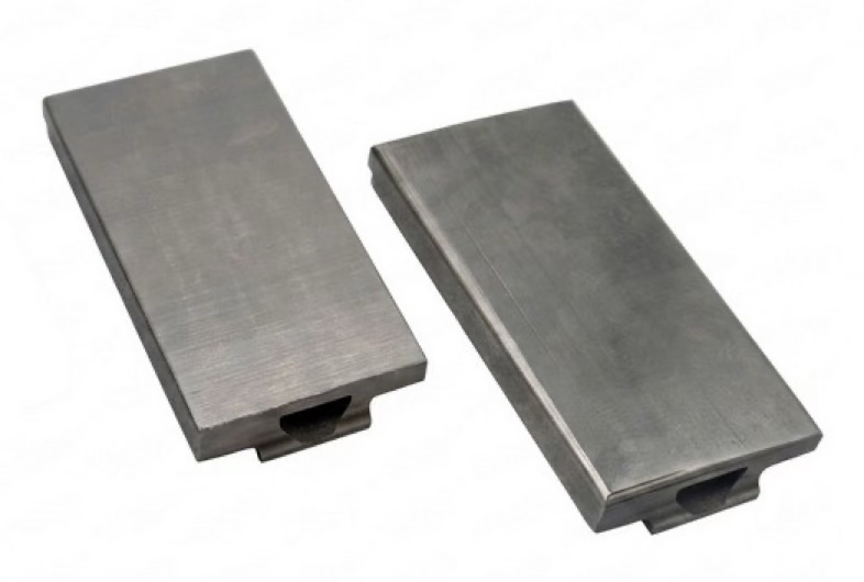
Finished flat and domed tungsten tiles with mirror-like plasma-facing surfaces, ready for installation in DIII-D.
The tiles were mounted on copper-alloy pedestals and installed in DIII-D's lower divertor in July 2026. Mehalick traveled to San Diego for the installation and participated in the experiments.
Over the course DIII-D’s Tile Testing Campaign, the AM tiles saw 3 days of direct plasma exposure. 74 of these plasma discharges were in high-confinement "H-mode" at medium-to-high power, for about four minutes of total plasma exposure.
"As far as we could tell in the control room, your AM tiles performed really well," Coburn told the team after the campaign.
A neighboring conventional tile that was slightly out of alignment melted along its leading edge and spattered onto one of the printed tiles, giving the team an unplanned look at how the printed material responds.

The divertor shelf before plasma exposure, with the printed flat split tile pair at center. [Photo credit: Ryan Hood, SNL]

After exposure: the printed tiles survived intact. Marks from the misaligned neighboring tile's melted edge are visible nearby. [Photo credit: Ryan Hood, SNL]
The tiles are now being removed, imaged and surface-scanned to compare with their condition before exposure. After a radiation survey, they will return to NC State for detailed analysis.
The project was presented at the AM2F 2026, the Additive Manufacturing and Advanced Materials in Fusion conference (https://am2f2026.psfc.mit.edu/) in Cambridge, Mass., on Aug. 31. In September, printed tungsten tiles from the project were on display at JEOL's booth at IMTS 2026, the International Manufacturing Technology Show, in Chicago.
"Fusion is moving fast. Qualifying new materials and manufacturing methods requires fusion-relevant data," Laggner said. "By exposing additively manufactured tungsten in DIII-D, we are generating that data on survivability and erosion."
"DIII-D lets us put candidate materials in front of a real fusion plasma and see what happens," Dr. Chris Ledford from ORNL said. "Seeing additively manufactured tungsten go from small test buttons to full-size tiles in the divertor in less than a year is remarkable, and the data from this campaign will help guide how tungsten components are designed for ITER and beyond."
Students at the center
"Our students and Post-docs drove this effort home," Horn said. "Aaliyah's earlier plasma tests are the reason DIII-D asked us in the first place. Olivia, an undergraduate, took these tiles from rough prints to finished parts sitting in a national fusion facility, then participated in the control room while they were tested. That's an experience most students never get."
Mehalick and Zuniga both study fusion from the plasma physics side, Mehalick as an undergraduate and Zuniga as a Ph.D. student in nuclear engineering. Neither came in as a manufacturing specialist. Both took the initiative to learn to run the wire EDM, grinding and characterization equipment at CAMAL, with training from Zhang, so they could see the project through themselves.
"In my classes, the wall of a fusion reactor is a boundary condition in an equation," Mehalick said. "This project made it a real part I had to cut, grind and measure. Learning to run the manufacturing equipment at CAMAL, and then monitoring these tiles during the plasma exposure with cameras from the DIII-D control room, changed how I think about what it takes to actually build a fusion machine."
"Our first DiMES samples would fit on a fingertip, so seeing that work lead to full-size tiles in the same machine less than a year later has been amazing," said Zuniga, who interned at ORNL this summer. "Spending the summer at Oak Ridge also showed me how much universities, national labs and industry depend on each other to move fusion materials forward."
The team
Name
|
Organization
|
| Tim Horn |
NC State, Mechanical and Aerospace Engineering; CAMAL |
| Florian Laggner |
NC State, Nuclear Engineering |
| Haozhi Zhang |
NC State, Mechanical and Aerospace Engineering (postdoctoral researcher) |
| Aaliyah Zuniga (Ph.D. student) |
NC State, Nuclear Engineering |
| Olivia Mehalick (undergraduate) |
NC State, Nuclear Engineering |
| Yutai Kato |
Oak Ridge National Laboratory |
| Michael Kirka |
Oak Ridge National Laboratory |
| Christopher Ledford |
Oak Ridge National Laboratory |
| Ezekial Unterberg |
Oak Ridge National Laboratory |
| Zane Marek |
JEOL USA, Inc. |
| Jonathan Buckley |
JEOL USA, Inc. |
| Satoshi Ono |
JEOL Ltd., Japan |
| Akimine Hatsuda |
JEOL Ltd., Japan |
| Jonathan Coburn |
Sandia National Laboratories |
| Florian Effenberg |
Princeton Plasma Physics Laboratory |
| Tyler Abrams |
General Atomics / DIII-D |
| Karl Schultz |
General Atomics / DIII-D |
| Kyle Teixeira |
General Atomics / DIII-D |
Funding
This material is based upon work supported by the U.S. Department of Energy, Office of Science, Office of Fusion Energy Sciences, using the DIII-D National Fusion Facility, a DOE Office of Science user facility, under contracts DE-FC02-04ER54698, DE-AC05-00OR22725 with UT-Battelle LLC, DE-NA0003525 with NTESS under DOE NNSA, and DE-AC02-09CH11466. Tile fabrication was funded by ORNL's Fusion Materials Core Program.
Disclaimer
Disclaimer: This report was prepared as an account of work sponsored by an agency of the United States Government. Neither the United States Government nor any agency thereof, nor any of their employees, makes any warranty, express or implied, or assumes any legal liability or responsibility for the accuracy, completeness, or usefulness of any information, apparatus, product, or process disclosed, or represents that its use would not infringe privately owned rights. Reference herein to any specific commercial product, process, or service by trade name, trademark, manufacturer, or otherwise does not necessarily constitute or imply its endorsement, recommendation, or favoring by the United States Government or any agency thereof. The views and opinions of authors expressed herein do not necessarily state or reflect those of the United States Government or any agency thereof.