In-situ Observation of Microstrain using SEM-EBSD and Tensile Testing
- |
- 2 MIN READ |
- 1274 |
- February 9, 2026 |
- Applications, Sample Preparation |
-

SM2025-03
Products Used: Scanning Electron Microscope (SEM), In-situ Tensile test, Electron Backscatter Diffraction (EBSD)
Introduction
SEM combined with EBSD enables detailed analysis of grain size, crystal orientation, and microstrain in materials. Using an in-situ tensile stage inside the SEM allows real-time observation of the material behavior under mechanical stress. This application note reports dynamic changes in copper grains during tensile testing.
Experimental Setup
We used the JSM-IT800SHL with an in-lens Schottky Plus electron gun, providing the high probe current needed for EBSD. The EBSD detector was Velocity Ultra (EDAX), and tensile testing was performed using the TS-1500 stage (TSL Solutions), capable of up to 1500 N (Figure 1). The specimen was a dog-bone shaped copper C1020P (1/2H), 1.0 mm thick. After polishing to a 1.0 µm diamond finish, it was annealed at 500°C in air to remove residual strain. Wide-area planar surface milling was performed using the IB-1954CP CROSS SECTION POLISHER™ to remove surface strain and oxide layers without adding stress.
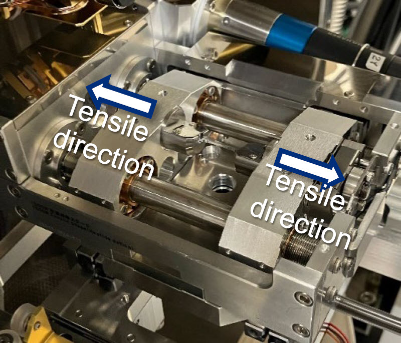
Figure 1. Appearance of the tensile testing stage mounted on the JSM-IT800 SEM stage
Tensile EBSD Analysis of Copper
Tensile testing was performed on a Cu specimen to evaluate its behavior up to fracture. Figure 2 shows the load-displacement curve, indicating that the specimen underwent elastic and plastic deformation before fracturing. SEM images taken just before and after fracture are shown in Figures 2(a) and 2(b). A QR code is provided to view a video capturing SEM images throughout the deformation process, where changes in the copper microstructure can be observed. SEM imaging and EBSD analysis were conducted at five displacement stages: 0%, 5%, 12%, 20%, and 36%. EBSD measurements were performed at x750 magnification, 20 kV accelerating voltage, and 70 nA beam current. A 150 µm x 150 µm area was scanned with a 0.1 um step size at 2000 pps. Figure 3 shows the SEM images, IPF (Inverse Pole Figure) maps, and KAM (Kernel Average Misorientation) maps corresponding to each displacement stage. The SEM images reveal that slip deformation had already initiated at the 5% displacement stage and progressed with increasing strain. IPF maps show changes in crystal orientation, with increasing color gradients within grains as deformation increases. KAM maps, which represent the average crystal orientation, with increasing color gradients within grains as deformation increases. KAM maps, which represent the average misorientation between neighboring pixels, highlight local orientation changes. High KAM values were observed nrear grain boundaries, suggesting a significant increase in dislocation density in these regions compared to grain interiors.
This study demonstrates that in-situ tensile testing combined with SEM imaging and EBSD mapping enables continuous observation of crystal orientation changes at the microscale.
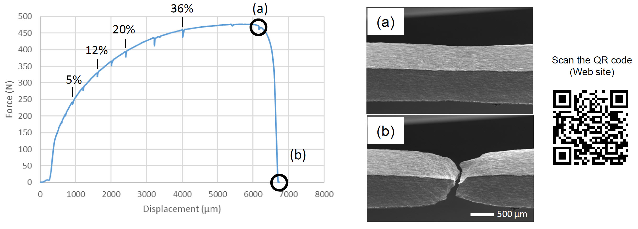
Figure 2. Load-displacement curve and low-magnification SEM images of the copper specimen: (a) just before fracture, (b) after fracture.
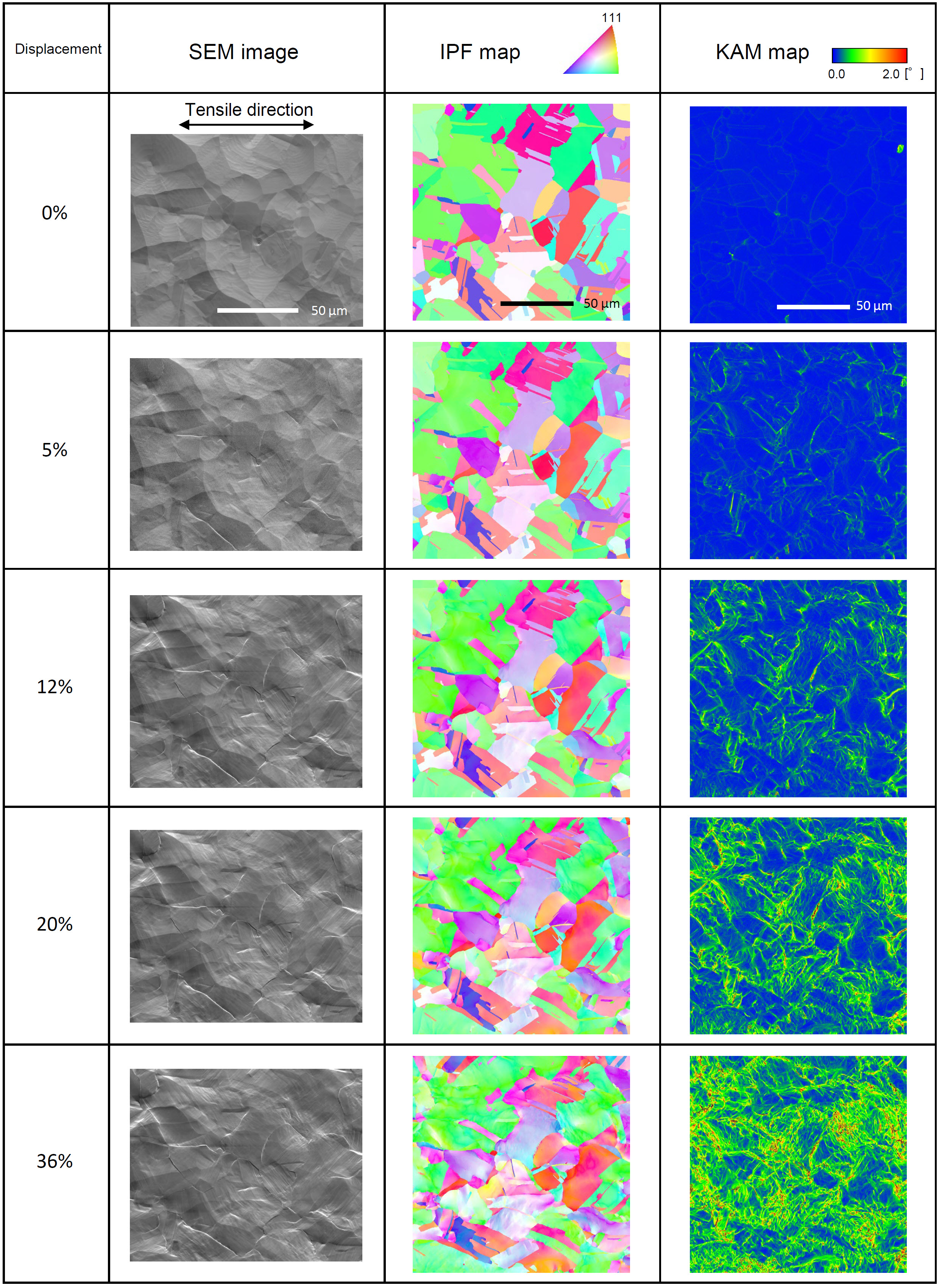
Figure 3. SEM images, IPF maps, and KAM maps at displacement levels of 0%, 5%, 12%, 20%, and 36%.