 Peabody, Mass., May 19, 2006 -- JEOL, the industry-leading manufacturer of high resolution Scanning Electron Microscopes (SEMs), will showcase its automated, 360 degree wafer edge review SEM in Booth 1101 in the South Hall at Semicon West 2006, Moscone Center, San Francisco.
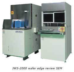
The JEOL JWS-2000 (200mm) and JWS-3000 (200/300mm) are the only wafer edge review SEMs that allow pinpoint inspection at any position on the circumference of the 200mm or 300mm wafer. A unique high tilt, full rotation stage makes it possible to rapidly review defects on the wafer’s edge in 1/10th degree increments.
Drive to any location on the wafer edge
“If you have identified a killer defect at 48.3 degrees (respective to the notch), or delamination at 68 degrees, the only way to see these defects is on the JEOL JWS because it’s the only system that has full automated rotational ability,” says Zane Marek, JEOL Semiconductor Equipment Product Manager. “We can drive to any location on the wafer edge. We also translate x/y coordinates from optical inspectors to theta-corrected positions to facilitate Wafer Edge ADR, which can accommodate Auto-EDS as well. These are all unique features available only through JEOL’s JWS lineup.”
 Wafer tilt feature
Another unique feature of the JWS-2000 is the wafer stage which can be tilted between 0 and 60 degrees, “making it possible to see the entire bevel and even a little below,” says Marek. The 300mm system features 0 to 45 degree tilt. The JWS system’s unique electron optics with high depth of field allows the wafer bevel and exclusion zone areas to be in focus at the same time.
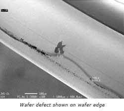
Edge defects can have hidden impact on yield
Wafer edge review is rapidly becoming accepted as an important step in identifying defects such as peeling films, residual slurry, cracks, chips, and particles on a thin circumferential area that can have a hidden impact on yield. “While traditional inspection methods rapidly identify a sub-100nm defect on the wafer surface, without edge review you will not be aware of that 5 micron defect on the wafer edge,” warns Marek.