Peabody, Mass., June 16, 2005 – JEOL will present a suite of solutions for critical analysis of wafer defects and nanometric designs at Semicon West 2005. From precision sample preparation to ultrahigh resolution imaging at the nanoscale, JEOL semiconductor tools are designed for today’s most advanced processes.
 Cross Section Polisher Sample Preparation
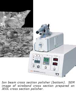
On display in the Final Manufacturing section of Semicon West is JEOL’s new cross section polisher for scanning electron microscope (SEM) sample prep. The JEOL CP slices and polishes difficult composite samples and coatings. These include solder bumps, PWBs, amalgams, thin films, intermetallics, and wire bonds. Using an argon ion beam, the CP preserves structures, voids and adhesions, interfaces, and coatings without deformation. It allows observation of crystalline structures and produces large area samples. Samples are ideal for EBSD observation with the SEM.
Ultrahigh Resolution SEM Imaging at up to 1,000,000X Magnification
Both cross section samples and full-size wafers can be imaged using JEOL’s ultrahigh resolution SEM, the JSM-7401F, which produces high contrast, high clarity images -- 1.5nm resolution at 1kV – at magnifications up to one million times. The new cold field emission SEM introduced this year features a unique Gentle Beam method that decelerates incident electrons, enhancing observation of nanometric structures.
For routine SEM observation, JEOL offers a family of high resolution electron microscopes for large sample sizes. 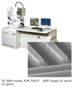 The high end model, large chamber JSM-6480LV offers 3nm resolution, pushbutton imaging, and an asynchronous 5-axis stage. The JSM-6380LV and the JSM-6060LV offer lower cost, smaller chamber solutions and flexible configurations.
Focused Ion Beam Sample Prep/Unmatched TEM Technology
For advanced cross section analysis requiring the highest performance TEM technology, the JEM-2500SE scanning transmission electron microscope (STEM) is simpler to use than an in-lens SEM, yet produces images with ultrahigh resolution – 0.2nm – up to five times the resolution of SEM tools. The JEM-2500SE is used to investigate the internal structures of devices with advanced power and optics. The STEM’s compact footprint and ergonomic design make it an ideal choice for the semiconductor fab.
For rapid production of cross section specimens for the STEM, JEOL represents the Seiko SIINT fully-automated focused ion beam (FIB) system that prepares and finalizes multi-point specimens at specified locations on 150, 200, or 300mm wafers without operator attendance. Using a gallium ion beam, the SMI 3050, 3200, and 3300 model FIBs rapidly and precisely convert the specified cross section area into a 100nm layer without destroying the wafer.
ADR SEM Enables Bare Wafer and Edge Review at Wide Tilt Angle Range
The JWS series of ADR tools offer high resolution, high throughput, and high tilt angles that enable imaging and detailed analysis of both bare and patterned wafers without the need for cleaving. Furthermore, these advanced systems enable comprehensive and automated wafer edge review, and auto defect classification that streamlines more than 60 classification codes, reducing rule writing and engineering time.
Visit JEOL at Semicon West 2005
JEOL will showcase the ADR with wafer edge review at Semicon West 2005, July 12-14, Booth #1101 South Hall of the Moscone Center in San Francisco. Analysis tools for back end processes will be showcase in Booth #7221 in the West Hall, Level 1.