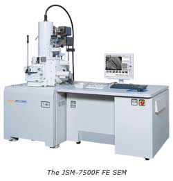
 Peabody, Mass., May 17, 2006 -- JEOL USA, a leading manufacturer of electron microscopes and analytical instruments, introduces a new ultra-high resolution Field Emission Scanning Electron Microscope (SEM) with advanced optics that clearly reveal intricate surface details during observation of nano structures of medical, biological, materials science, and semiconductor samples.
Unique in-lens performance with semi-in lens advantages
The performance and stability of the new JSM-7500F allows specimens to be easily observed at magnifications up to 1,000,000 X with a resolution of 1.4 nm at an accelerating voltage of 1kV. The first SEM of its kind to demonstrate in-lens performance without associated cost or sample size restrictions, the JSM-7500F achieves 0.6nm resolution at 30kV and accommodates samples up to 200mm in diameter.
Observe fine surface morphology of nano structures
The JSM-7500F features a patent-pending low angle backscatter electron detector (LABe) that dramatically reduces charging, resulting in enhanced surface detail and compositional contrast. The FE SEM’s Gentle Beam (GB) mode allows spectacular image resolution at accelerating voltages down to 100V, reduces sample contamination, and suppresses charge buildup. This enables the user to extract pure surface information from the specimen. The new r-filter lets the user freely select the energy range of detected secondary and backscattered electrons, providing four modes of image contrast: composition, topography, or a mix of the two.
Automation featuring simultaneous image acquisition
The JSM-7500F enables simultaneous, on-screen comparison of up to four live images from a variety of detectors, including in-lens SE, in-lens BE, below lens BE (topo, compo), and LABe.
The JSM-7500F is efficient and simple to operate, allowing routine, optimized functions to be automated. The standard eucentric five-axis specimen stage is precisely controlled via standard trackball, touchpad, mouse, and knobset. An autoloader specimen exchange airlock chamber is available for 8” samples. Image saving and report creation are intuitive, and 16-bit depth imaging produces bright, clear images.
Designed for efficiency and stability
An environmentally-friendly SEM, the new Economy Mode (stand-by with scheduling) can save from 25% to 55% in energy consumption.
This cold-cathode field emission SEM is highly resistant to floor vibration and acoustical interferences found in cleanroom environments and less-than-ideal settings. It features a large and versatile chamber with ports for several attachments such as EDS, EBSD, STEM, CL, IR-camera, EBIC feedthrus as well as the in-lens SE and BE, below lens SE and BE, and the new LABe detectors. A dry vacuum system features a turbomolecular pump as standard.
Ultimate imaging with total clarity
The JSM-7500F enables advanced imaging in the fields of metals, minerals, semiconductors, biology, materials science, and nanotechnology. No other single FE SEM produces this level of high resolution at high kV (0.6nm @ 30kV) and at low voltage (1.4nm @ 1kV) with selectable surface morphology and compositional contrast.