 April 28, 2009 (Peabody, MA) -- For now, scientists at Florida State University (FSU) can only envision what some misoriented atoms are up to along the defects of the new materials that they are developing. They’ll finally be able to clearly see each individual atom and how it relates to its neighbors when they take delivery of a new JEOL atomic resolution Scanning Transmission Electron Microscope (S/TEM) later this year.
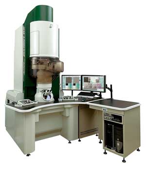
FSU’s Applied Superconductivity Center, housed in the National High Magnetic Field Laboratory, the High Performance Materials Institute in Tallahassee, Florida, scientists at FSU, and even more broadly throughout Florida, will soon have access to the highest resolution – 80 picometers, or one-trillionth of a meter – of any commercially available S/TEM in its class. The imaging and analytical resolution of the new JEOL 200kV S/TEM will make it possible to directly observe atomic position, chemical composition, and electronic bonding information that is crucial to development of novel materials with the highest performance. Typical materials are superconductors, light weight high performance composites, semiconductors, biomaterials, catalyses, materials for fuel cells and high strength metallic materials.
“It’s great that multiple fine institutes and centers exist on this campus and can agree to collectively invest on behalf of a large number of people,” said Dr. David Larbalestier, one of the world’s foremost materials scientists and director of Florida State University’s Applied Superconductivity Center. “I have an intense interest in high temperature superconductors and hope to use this new instrument to drive superconducting technology forward. Last year with our colleagues in the magnet lab we demonstrated that these new superconductors could be used to generate magnetic fields fifty percent higher than ever before by any superconducting magnet. It’s very exciting.” Other practical applications for the new superconductors include high power underground power cables that have the potential to greatly enhance the transmission of power underground into big cities. “But to have such a capable instrument with broad capabilities means that it can be very useful to many other leading campus researchers too.”
Researching the properties of powerful new superconducting materials, such as YBCO, BSCCO, and the recently discovered pnictides at FSU’s National High Field Magnet Lab (NHFML), includes testing them with the world’s strongest magnets. The NHFML is home to hybrid and high field magnets including one with the world’s highest magnetic field, 45 tesla, nearly a million times that of the earth in its orbit.
“Advanced superconductors are true nanostructures,” said Labarlestier. “When I was a young assistant professor, we were trying to understand the workhorse of 95% of all superconducting applications, niobium titanium, and we got our first glimpse of the nanoribbons of almost pure titanium, only 2-3 nm thick that are so essential to their outstanding properties. We were convinced we needed an analytical microscope and bought one of the very first fully analytical machines from one of JEOL’s competitors. This new JEOL STEM in full analytical mode will let us perform analysis at the single atom level that we dreamed of then, but which has been out of our grasp until now. The new machine is ideal for settling this type of problem.”
The High-Performance Materials Institute (HPMI) will utilize the TEM in its efforts toward developing multifunctional nanocomposites. The advanced nanomaterials should one day be used to produce lighter, stronger and safer aircraft, spacecraft and automobiles. “This resource should prove vital toward accelerating nanocomposites into the market place,” said Dr. Richard Liang, Chief Technologist of the HPMI and Professor of Industrial and Manufacturing Engineering. “We should soon provide the capabilities to produce multifunctional materials that will make transportation more energy efficient, affordable, and safer.”
“We will be able to probe individual atomic sites and determine the atomic and electronic structure with single-atomic column sensitivity,” Dr. Yan Xin, Associate in Research, Magnet Science & Technology, explained. “For instance, various defects, such as dislocation sites, in materials are a major factor to impact the applications of high temperature superconductors, high strength materials, biomaterials, semiconductors and fuel cell materials. We are working to improve defect properties so it’s very important to know exactly the position and chemistry of individual atomic column. This sub-angstrom microscope will give us that information one atomic column by one atomic column.”
The funding for the TEM was provided by the Florida State University Research Foundation, with matching funds from the Center of Excellence in Advanced Materials. The Center of Excellence, funded by the Florida Board of Governors, was established by researchers at the High-Performance Materials Institute.