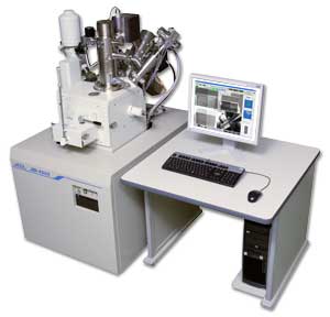
 November 27, 2007, Peabody, Mass. -- JEOL USA introduces a new high throughput SEM/FIB that combines Focused Ion Beam micro milling with the high resolution imaging of the JEOL LaB6 electron column. The MultiBeam is a high-productivity tool for IC defect analysis, circuit modification, TEM thin film sample preparation, and mask repair.
A versatile all-in-one system, the MultiBeam features Serial Slicing and Sampling (S3™) for in-process monitoring of milling, fabrication, and reconstructing 3D images of the sectioned area. A maximum milling current of 30 nA ensures high throughput milling of large areas.
Additional features include low vacuum operation for non-conductive specimens without coating or alteration, a gas injection system for etching and deposition, a large stage for up to 150 mm samples, and a multiple port design for a range of analytical needs. Samples are loaded through a standard airlock system.
Two new nano-imaging labs will take delivery of the MultiBeam systems in early 2008. JEOL USA has formed a partnership with both the University of Southern California and Boston College which will advance applications research on the east and west coasts.
For more information visit www.jeolusa.com/tabid/496/Default.aspx.