Ion beam sputter coating with CROSS SECTION POLISHER™
- |
- 1 MIN READ |
- 4596 |
- February 19, 2021 |
- Sample Preparation |
-

Utilize your CP for sputter coating
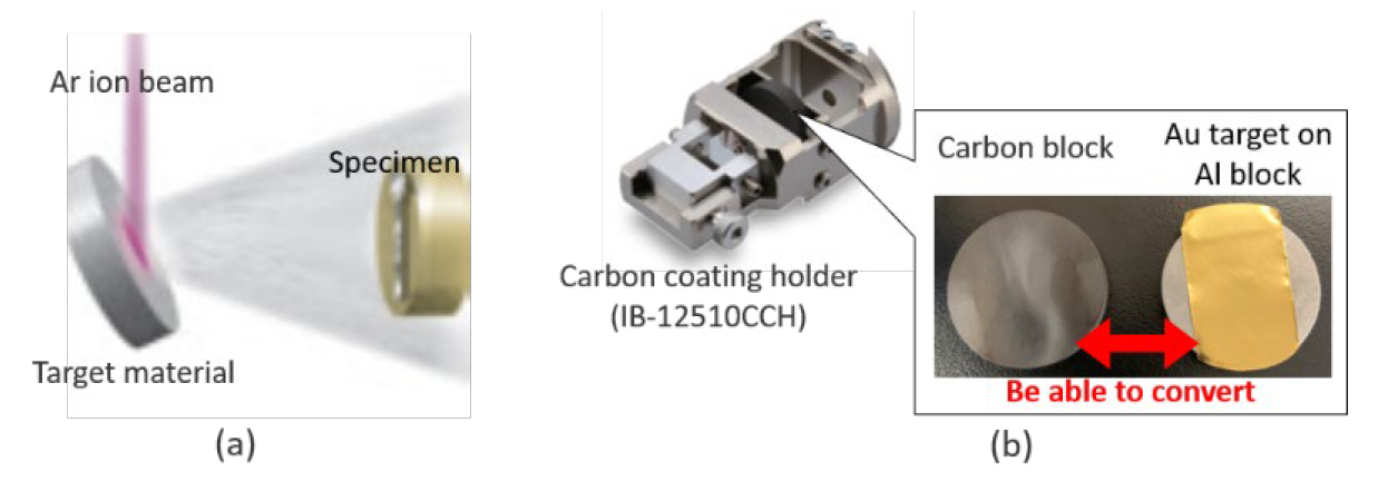
CROSS SECTION POLISHERTM (CP) is an SEM specimen preparation device that utilizes a broad Ar ion beam to produce artifact-free cross-sections. The same principle can be employed not only for ion-milling but also deposition of thin layer to the specimen surface, in particular, conductive coating for followup observation of a non-conductive specimen in an SEM. Figure 1(a) shows the principle of ion beam sputter coating. The target material is irradiated by the ion beam, instead of the specimen, creating a cone of sputtered material that is deposited on the specimen surface in a form of thin conductive coating. Figure 1(b) shows the carbon-coating holder (IB-12510CCH), that uses a carbon planchette as a target. Typically, this holder is only for the carbon coating; however, it can also be used for metal coating, simply by attaching a Au/Pd or other metal target (example shown is Fig. 2).

Figure 1: Schematic of ion beam sputter coating by CROSS SECTION POLISHER™ (CP). (a) Principle of ion beam sputter coating, (b) Coating holder and targets.

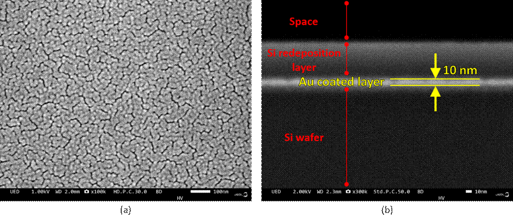
Figure 2: Gold coating results. (a) Au coated area on Si wafer. (b) Cross section image of Au coated layer made by CP.
Figure 2 (a) shows the surface image of gold coated area on Si wafer. Coating condition is accelerating voltage 6 kV, irradiated ion current 130 µA and process time 3 minutes. Figure 2(b) shows the cross-section image of gold coated layer made by CP. The resulting coating thickness is 10 nm gold layer on Si wafer. This uniform layer provides good electric conductivity.
The advantages of this method:
- No need for a dedicated sputter coater. CP can perform both polishing and coating.
- Adjust layer thickness by changing accelerating voltage and process time.
- Both carbon and metal thin layer can be deposited.