Imaging a Spider Web with the SEM
The challenge was to image the spider’s web without causing any induced stress or deformation of the structure as collected. The web was collected between two glass plates to protect the structure. The top glass plate was removed, and the sample was transferred to an SEM holder that was configured as in the Photos.
Top reference holder with cap removed.
Top reference holder with carbon tape on the cap and with cap reinserted.
Top reference holder with tape pressed onto the web.
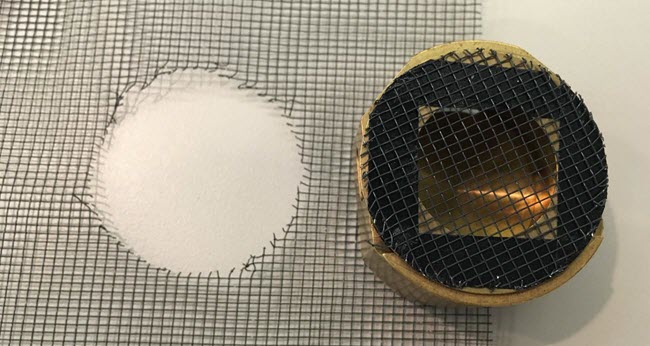
For illustration purposes a piece of window screen was used to demonstrate this technique, as spider silk would be too small to show up in the macro photos. A strip of conductive C tape was applied to completely surround the removable cap of a holder designed to hold polished metallographic mounts. This was then pressed onto the web and lifted off. This allowed the intact web inside the tape to be ripped away from the rest of the web outside of the tape without any stress or strain. The cap was then placed onto the specimen holder for insertion into the SEM. This type of mounting allows the microscopist to have nothing in the background of the image.
Top reference holder with tape pressed onto the web.
Top reference holder with tape lifted from the web.
Vivamus sagittis lacus vel augue laoreet rutrum faucibus dolor auctor. Duis mollis, est non commodo luctus.
Top reference holder with web firmly attached showing the remaining web left behind.
In addition to preserving the structure the goal was to create a publishable image. This is often as much art as it is science. One of the main components of such an image is a very clean, featureless, completely black background. The second attribute of a high-quality image is to have as little artifact in the image as possible. Two of the most common artifacts in SEM images, especially on organic or other low atomic number materials are edge effect and charging. Edge effect is a washing out of edges, corners or small surface structures due to electron emission from a large volume of excitation between the electron beam and the sample that greatly reduces true surface morphology. This is easily overcome by lowering the accelerating voltage. With older SEMs, this meant loss of resolution, but with today’s FEG SEMs there is effectively no loss in resolution when operating at low kV.
The other artifact is charging which is a buildup of primary beam electrons on the surface of a nonconductive sample. In the past a conductive coating (either evaporated carbon or sputtered metal, typically Au, Pd, or Pt) had to be applied to make the sample conductive. Today’s FEG SEMs, with ultra-high resolution, are capable of imaging the grain structure of any metal film which has a subtle surface morphology that is not really present in the real sample. A charging sample prohibits low energy electrons, which carry surface morphology information, from escaping from the surface. This too can be eliminated at low accelerating voltages without the need to apply a coating thereby simplifying and speeding up the analysis process. The resulting images were used for the presentation at M&M 2016 and one was chosen as the cover photo for the journal BioNanoScience Vol.6, No.2, June 2016.