Automation of High‑Magnification Observation of NMC Cathode Active Material Particles Using an SEM External Control API and Python®
Introduction
For stable battery performance, it is essential to control the surface condition and particle shape of NMC (lithium nickel manganese cobalt oxide), which is used as a cathode active material in lithium‑ion rechargeable batteries. However, operators must manually measure large numbers of NMC particles and observe their surfaces at high magnification with scanning electron microscopes (SEMs), which requires significant time and effort. Recent SEMs are equipped with fast and accurate automatic contrast/brightness (ACB), auto focus (AF), and auto astigmatism correction (AS). They also provide external control APIs, allowing users to develop their own automation programs. In this study, to address the issues above, we automated high‑magnification observation of NMC particles by using the SEM external control API and Python®, based on an optimized sample preparation suitable for automatic measurement.
SEM automation with API and Python®
API for external control has been released to allow SEM operation using Python® or C#. Therefore, SEM routine workflows can be automated according to each research or observation purpose. In Python®, packages such as OpenCV, which is suitable for image processing, and matplotlib, which is useful for graph drawing, are available and easy to use. By combining these tools, it is possible to automate the entire process, including SEM operation, image analysis, graph creation, and report generation.
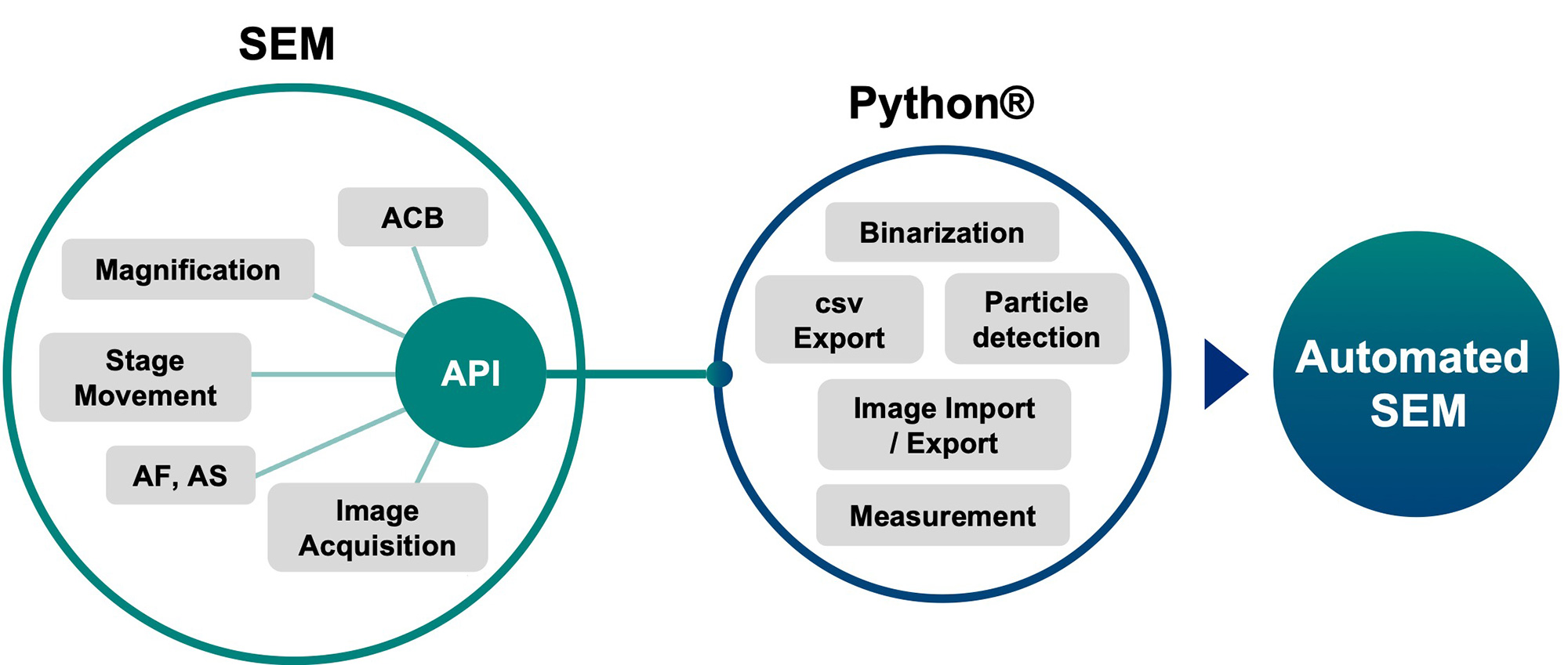
Integration of SEM External Control API and Python® for Automation
Sample preparation and substrate evaluation
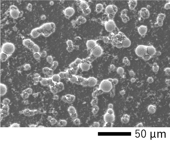
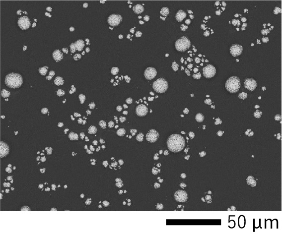
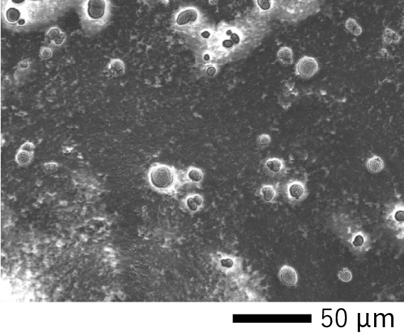
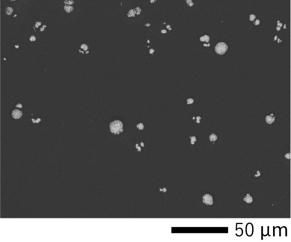
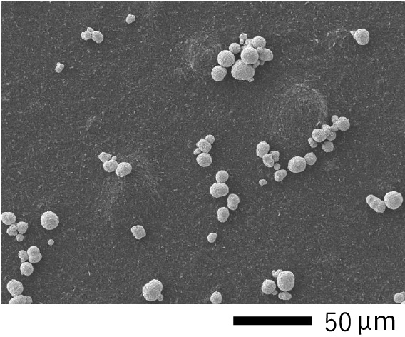
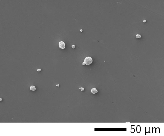
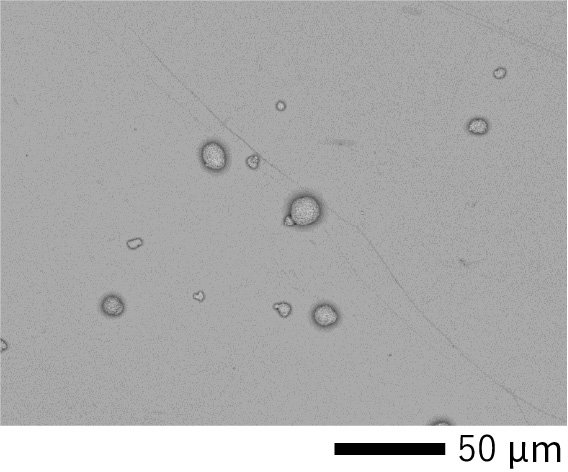
Sample preparation greatly affects the accuracy of automatic adjustment and particle detection during automated observation. Therefore, we evaluated the substrate on which the sample is placed based on whether the substrate does not cause charging, provides sufficient contrast for binarization, and offers high throughput with good reproducibility. The NMC powder particles were dispersed in the preparation solution and dropped onto the substrate. As the preparation solution, we selected ethanol because it dries quickly and has high hydrophilicity. For the SEM conditions during comparison, we used a probe current of 400 pA and a landing voltage of 5 kV. The threshold for binarization was determined using the cv2.threshold function, which performs Otsu’s binarization [1] via the OpenCV library.
| |
Secondary Electron Image |
Backscattered Electron Image |
Result |
| Carbon tape with Al substrate |
 |
 |
▲Charging of tape is observed in SEI image
●High compositional contrast
▲Deformation of the tape surface caused by ethanol is observed.
|
| Nonwoven carton tape |
 |
 |
▲Charging of tape is observed in SEI image
●High compositional contrast
▲Deformation of the tape surface caused by ethanol is observed
|
| Carbon paste |
 |
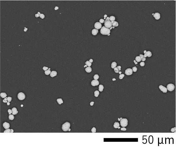 |
●No charging
●High compositional contrast
●Easy to use; it only needs to be applied to the substrate
|
| Si substrate |
 |
 |
●No charging
▲The contrast difference between particles and Si substrate is not visible in the BSE image
●The Si substrate is disposable and easy to handle.
|
*Python is a trademark or registered trademark of Python Software Foundation.
High magnification observation automation condition
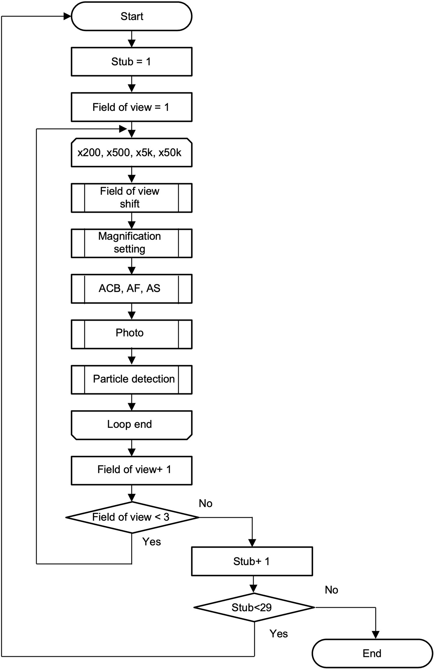
Flow chart of automation observation |
| SEM |
JSM-IT810SHL |
| Landing voltage |
5 kV |
| WD |
7 mm |
| Probe current |
400 pA |
| Detector |
SED (Secondary electron detector)
BED (Backscattered electron detector) |
| Sample |
NMC811 |
| Number of stubs |
29 stubs |
| Field of view ratio per stub |
3 field of views |
| Magnifications |
x200, x500, x5,000, x50,000 |
| Total number of acquired images |
696 |
| Python® |
Version 3.10.17 |
| OpenCV |
Version 4.11.0 |
| pythonnet |
Version 3.0.5 |
|
Experiment result
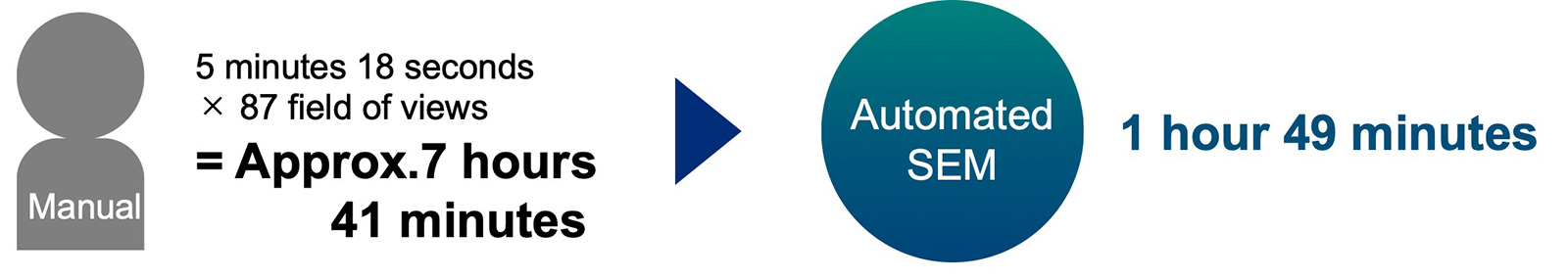
A total of 696 images from all 29 stubs were acquired in 1 hour, 49 minutes, and 17 seconds. It was confirmed that all images were captured with appropriate brightness, focus, and astigmatism adjustment. The secondary electron (SE) images and backscattered electron (BSE) images of a selected field of view at each magnification are shown below. Because the images were acquired while keeping the particle within the field of view even at high magnification, the fine structure of the NMC surface could be observed. The particle shape at ×5,000 and the surface morphology at ×50,000 were clearly visualized. In addition, the size and shape of the submicron primary particles were distinctly observed.
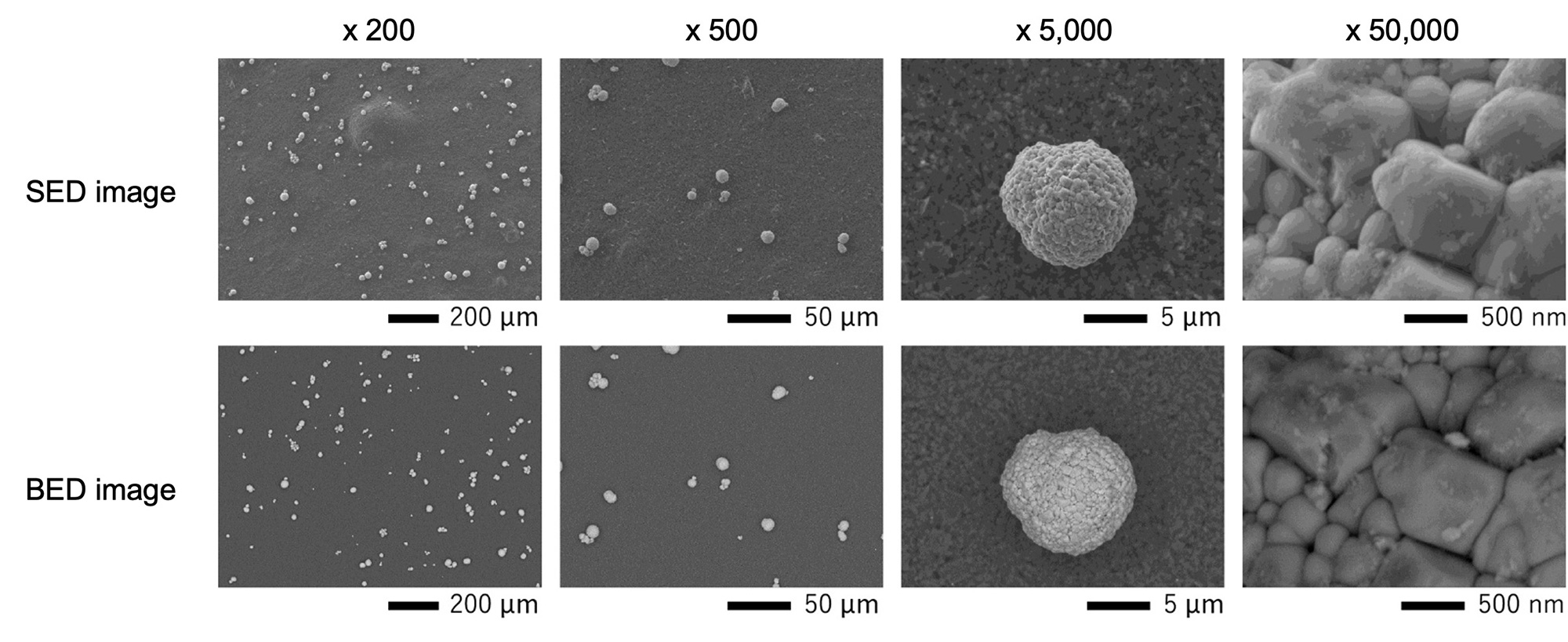
SEM image acquisition result from x200 to x50,000
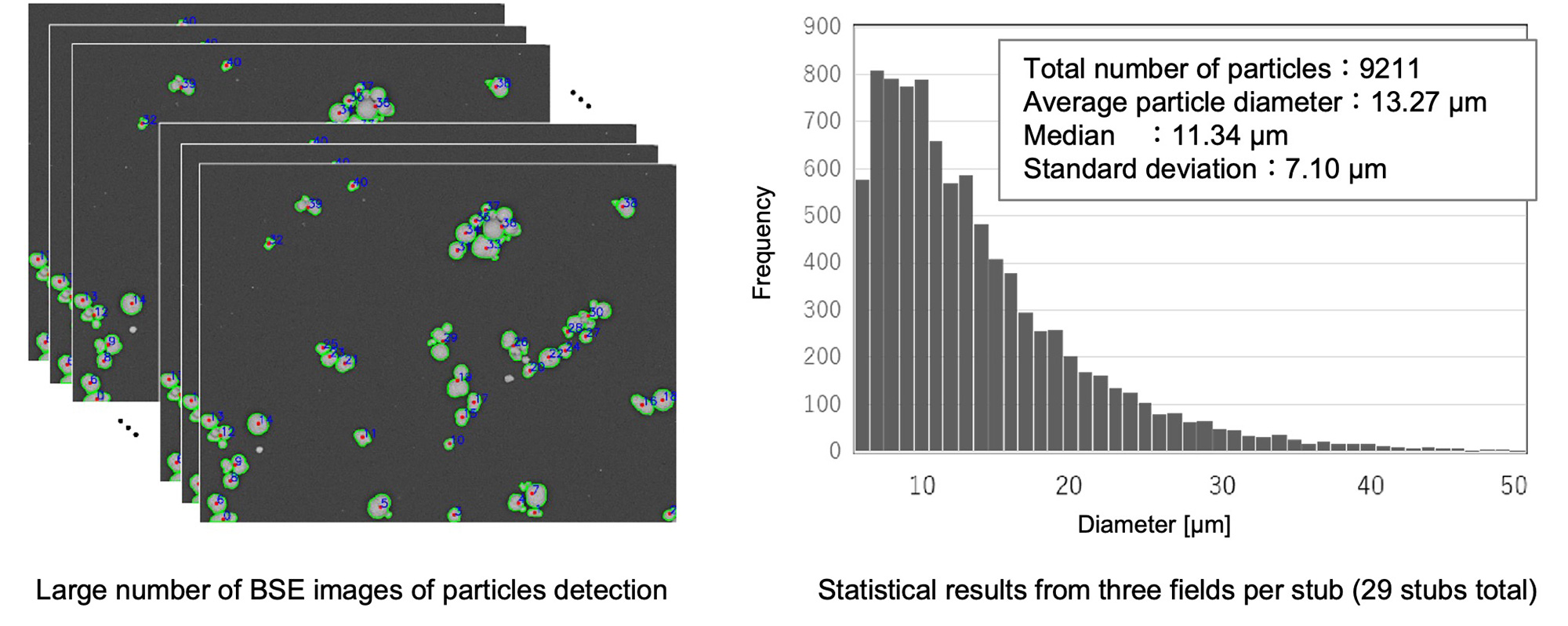
Using a backscattered electron compositional image at a magnification of ×200, the particle lengths in each field of view for each stub were measured simultaneously during observation. The measurement results from all fields of view across the 29 stubs were combined to calculate the particle size distribution and statistical values. The analysis quantitatively confirmed a broad particle size distribution, with a median size of 11.34 μm and a standard deviation of 7.1 μm.
When operators perform the same procedure manually, including sample preparation, it requires a full day. In contrast, the automated SEM not only completes the entire process in a shorter time but also allows the saved time to be used for other tasks during measurement.
Summary
We examined the preparation of samples and developed automated observation functions to enable the acquisition of large amounts of NMC particle data. It was found that carbon paste is suitable as a substrate material for mounting NMC particles. Furthermore, by combining an SEM external control API with Python®, we were able to construct a purpose‑specific automated SEM system. In the future, such customized automated SEM systems are expected to further improve efficiency in quality control and materials development, not only for NMC particles but also across various fields.
Reference
[1] Otsu, N. (1979). IEEE Transactions on Systems, Man, and Cybernetics, 9(1), 62–66.