JEOL Technical Note
The first commercially available SEM was introduced over 50 years ago and to this day there is still no internationally accepted standard for determining SEM resolution. To add to the confusion, each SEM manufacturer relies on their own sample and methods for determining resolution.
Two of the most common ways to determine resolution are by:
- Measuring the separation between two adjacent objects
- Collecting a line profile of the signal intensity changes across a sharp edge
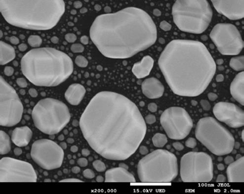
Figure 1: SEM Image of a gold on carbon test sample
JEOL has traditionally used a sample of small gold particles evaporated on a carbon substrate (Figure 1). With this type of sample, resolution is then determined by either measuring the separation between two adjacent gold particles or by evaluating the line profile of the signal intensity changes across a gold particle’s edge.
These techniques are subjective in nature. Defining the edge of a particle will be different from one person to the next based on how that person interprets or ‘sees’ the edge of a particle. When using the line profile method, the distance for the signal transition is considered to be related to probe diameter. JEOL uses the traditional convention and measures at the 84th and 16th percentile of the transition (1 sigma value). This is not true for all manufacturers and values of 75th/25th and 65th/35th percentile have been reported by other vendors. As can be seen in Table 1, this leads to lower reported values of resolution even from the same edge profile in an image. Clearly, resolution specifications cannot be compared easily today between different manufacturers.
| |
84% |
75% |
65% |
| Beam diameter (resolution) |
1.4 nm |
1.1 nm |
0.6 nm |
Table 1: Example showing the resolution determined from the same edge profile using three different percentiles to calculate the beam diameter.
Another layer of complexity is added with digital image acquisition in today’s SEMs. The pixel resolution of the final image has an impact on the smallest features that can be resolved, meaning that the resolution measurement is intimately linked to the pixel size. Consider an image taken at 100,000X with a field of view of 1.28 um. If the image pixel resolution is 1280 X 960, then we have a pixel length of 1 nm/pixel. To distinguish a probe diameter of 3 nm would require image information that could be observed across only 3 pixels. Taking the same image with an increased pixel density of 2560 x 1920 would mean that the same information could be observed across 6 pixels.

Figure 2: Line Profile Method for SEM Resolution
Since image acquisition and the actual measurement procedures can vary considerably between different microscope vendors, it is important to be mindful when relating and comparing resolution numbers. How the measurement is made and what sample and parameters are selected can have a profound impact on the resolution number reported.