Low Vacuum Secondary Electron Detector
The development of low vacuum scanning electron microscopes (SEM) created a need for an alternative secondary electron detector (SE) that operates at elevated pressures. The standard Everhart-Thornley type secondary electron detector cannot be used in low vacuum mode due to the high voltage applied on the detector for signal collection.
Our new generation of low vacuum secondary electron detector (LVSED) provides enhanced performance at fast scan speeds and even greater collection efficiency. Why choose LVSED imaging over backscattered electron (BSE)? Considering electron-beam sample interaction, SE imaging can provide better overall spatial resolution as well as the ability to observe fine topographic detail when compared to BSE imaging. This is especially true when imaging low Z materials where interaction volumes can be high with BSE imaging.
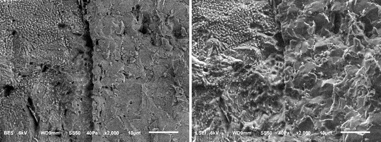
Figure 1: Pharmaceutical Tablet at Interface with Outer Coating – 6kV, 40Pa (BSE Image Left; LVSED Image Right)
Also, when dealing with heterogeneous samples that include a mixture of high and low Z components, compositional contrast can dominate with BSE imaging. Therefore, when there is also a need to observe fine topography, the LVSED will complement the information provided from the BSE image.
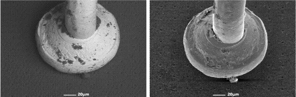
Figure 2: Wire Bond on Si at 15kV, 35Pa (BSE Image Left; LVSED Image Right)
The principle behind how our LVSED works is based on gas amplification. Secondary electrons emitted from the sample interact with an electric field and are accelerated toward the LVSED. In this process, the electrons interact with the gas in the sample chamber, generating more electrons and ions, thus amplifying the signal.
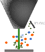
Figure 3: Principle of LVSED
Additional images below show further examples of LVSED Imaging.
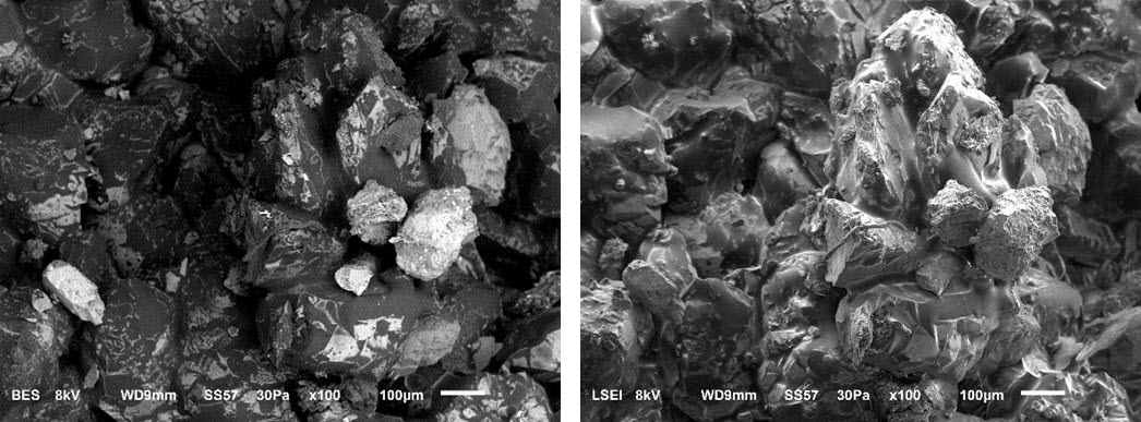
Figure 4: Crude Oil in Sandstone; 8kV, 30Pa (BSE Image Left; LVSED Image Right)
Cryo Images from Biological Samples

Figure 5: Vegetable Root; 15kV, 50Pa (left) Penium (SP); 10kV, 60Pa (right)