Sample Preparation Techniques – Conductive Coatings
In scanning electron microscopy (SEM), conductive coatings are commonly applied to the surface of insulating or beam sensitive materials such as biologic specimens, polymers, ceramics, geologic specimen, and semiconductors to dissipate charge build-up or reduce structural damage resulting from interaction with the electron beam. There are a wide variety of commercially available coating materials, including metals such as gold, platinum and iridium and non-metals including carbon. But which, if any, is right for you? Here we discuss when it is appropriate to add a conductive coating to insulating or beam sensitive materials and how to pick the best coating material for your applications.
DO I NEED TO ADD A CONDUCTIVE COATING?
Before you decide what type of conductive coating best suits your needs, it is important to assess whether a conductive coating is necessary. There are multiple reasons why you might choose not to coat your insulating samples. If the sample is high-value or needs to be used after SEM analysis, then you might not want to alter the surface. Similarly, it is difficult to apply an even conductive coating to samples with significant surface topography. For many applications, it is possible to collect satisfactory images and EDS data in low vacuum mode. Generally, there are two questions that we ask when determining whether to add a conductive coating to samples:
- Does this sample have a purpose after SEM analysis? If the answer is yes, then it is probably not a good idea to add a conductive coating. While most coatings can be removed either by mechanical polishing or with ionic liquids, these options may not be ideal or possible for your sample.
- Can I complete my imaging and/or chemical analysis at low KV or in low vacuum? Many insulating samples can be imaged at low accelerating voltages (0.5-3kV) in high vacuum mode. For those that cannot, or if chemical analysis (e.g., energy dispersive spectroscopy/EDS) is of interest, it may be possible to collect adequate data in low vacuum mode. By introducing air into the chamber, low vacuum mode dissipates charge build-up. For example, compare Figure 1A and 1B below. In 1A, the insulating sample is charging and impossible to image in high vacuum. In low vacuum, as shown in Figure 1B, the charge is dissipated, and it is possible to image the sample uncoated. However, introducing air results in beam spread, reducing both image quality (compare Figure 1B to 1C) and the accuracy of quantitative EDS data. So long as this tradeoff is acceptable, then it is not necessary to coat your samples.
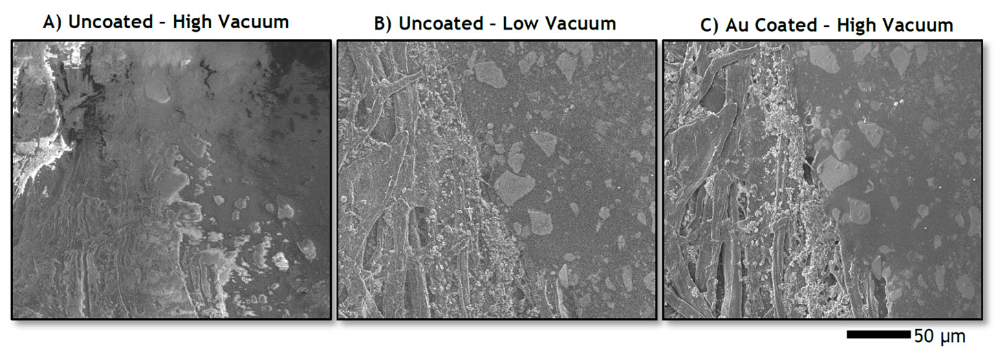
Figure 1. Organic mineral-filled ink on calcium carbonate-coated cellulose paper. Secondary electron images of an insulating material imaged A) uncoated in high vacuum mode, B) uncoated in low vacuum mode (LVHSED detector) and C) gold coated in high vacuum mode.
WHAT MATERIAL SHOULD I COAT WITH?
Now that you have determined that a conductive coating is necessary, the next step is to assess what type of coating best suits your needs. It is important to consider the type(s) of imaging and chemical analyses that you will be conducting as well as cost-benefit and ease of use. Metal coatings are ideal for high-resolution imaging. A metal coating will not only provide a conduction path but also aid in heat dissipation with beam sensitive samples. Metal coatings also provide a higher secondary electron yield which can improve signal to noise when imaging under high resolution (low probe current) imaging conditions. One disadvantage is the possibility of absorption of low energy X-rays or interference with X-ray lines inherent in the sample being analyzed when performing EDS analysis. In contrast, carbon is an ideal conductive coating for EDS analysis because its single detectable low-energy X-ray peak does not overlap with any other elements. Also, its low electron and X-ray absorption will allow for better backscatter electron signal and no interference for EDS analysis. However, care must be taken when adding a carbon coating as carbon evaporation is a high-temperature coating technique that can damage thermally sensitive samples. Ultrafine coatings for high magnification imaging and precise quantitative analysis require expensive high vacuum coating systems, while solutions ideal for lower magnification work are generally simple and cost effective. Although many solutions exist, including mixed metal coatings, the conductive coatings that we most commonly recommend include:
- Carbon: Carbon evaporation is a popular solution for performing quantitative chemical analysis (EDS, WDS, etc.). Unlike metals, carbon only has one detectable low-energy X-ray peak with no significant interferences and does not affect the specimen’s X-ray yield. However, if the sample is thermally sensitive (e.g., polymers), then the carbon evaporation process may damage the sample. In that case, a metal coating via sputter coating is recommended. Carbon does not require a high vacuum coating system, though for ultrahigh resolution imaging and accurate quantitative analysis (EDS, WDS) it is strongly recommended to ensure a fine and even coating.
- Gold: Gold sputter coaters are generally quick, easy to use, and inexpensive, making them a popular solution for low- to moderate-magnification imaging (<50,000x magnification). Gold works well for thermally sensitive materials like polymers. At magnifications greater than ~50,000x, the individual gold grains in the coating are visible so a finer-grained coating is recommended. Gold does not require a high vacuum sputter coater, though coating in high vacuum or in an Ar-purged system will result in a more even coating.
- Platinum: Sputter coating with platinum offers many of the same advantages of gold, but its finer grain size is better suited for high magnification imaging (50,000-200,000x). Platinum is the finest metal coating that does not require a high vacuum sputter coater, though coating in high vacuum or in an Ar-purged system will result in a more even coating.
- Iridium: Iridium has become a popular choice in recent years for ultrahigh resolution (>200,000x) imaging. Unlike other ultrafine metal coatings, such as chromium or tungsten, iridium does not oxidize. It is also a robust alternative to carbon coating for performing quantitative chemical analysis (EDS, WDS) on thermally sensitive samples or samples where quantifying carbon content is of interest. Iridium requires a high vacuum sputter coater.
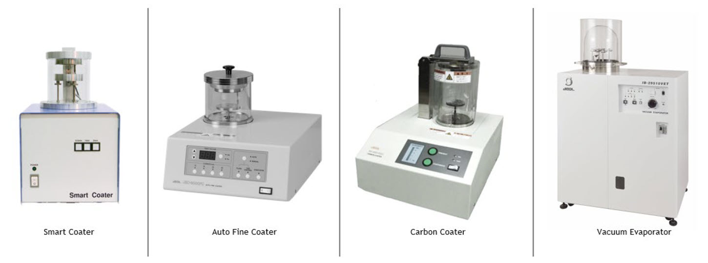
Figure 2. JEOL Coating Solutions
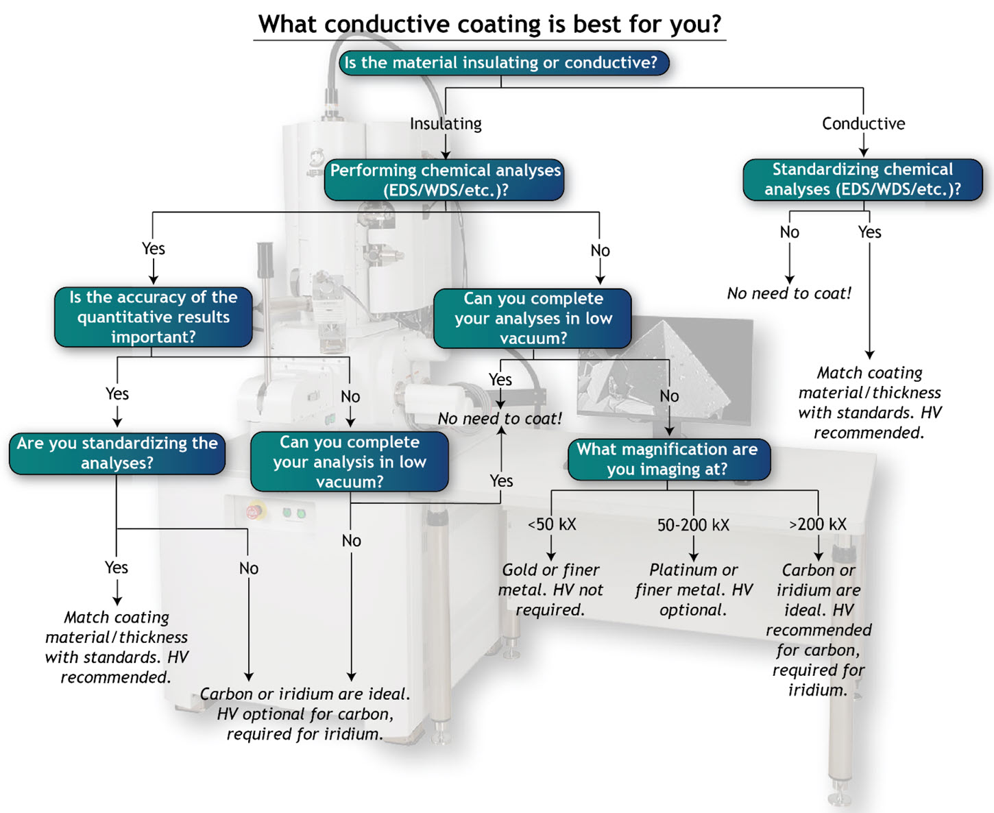
Figure 3. Generalized flow chart for conductive coatings. HV = high vacuum coater.