TTL system: Reduction of Effects of Lens Aberrations
Latest Innovation in our FE SEMs
SMART – POWERFUL – FLEXIBLE
Imaging of nanostructured materials requires a new design of SEM that provides ultimate resolution for both imaging and microanalysis, combined with the ability to image any type of material. An innovative new SEM column design from JEOL Ltd. utilizes a hybrid lens (combination electrostatic and electromagnetic lenses) in conjunction with a Through-The-Lens (TTL) detection system to provide the user with ultimate imaging and analytical performance. The hybrid electrostatic/electromagnetic lens minimizes magnetic field effects at the sample and is relatively impervious to stray magnetic fields. The lens is characterized by low values for the spherical and chromatic aberration coefficients. Moreover, the proven Aberration Correction Lens (ACL) technology automatically maintains small probe size for both imaging and microanalysis.
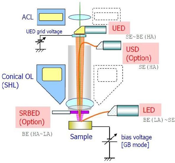
Figure 1: Schematic drawing of the TTL system
The new design provides the user with enhanced resolution at any accelerating voltage by effectively reducing the effects of beam aberrations (and particularly chromatic aberration at low accelerating voltages) on the spot size via two distinct mechanisms – beam booster within the electron column and beam deceleration at the specimen. The beam booster maintains high positive potential (e.g. 7 kV) throughout the final lens, regardless of the operating voltage selected by the user. The beam is then decelerated to its final landing energy. Since the beam energy E is always maintained at a high value, the transverse chromatic aberration (scales as αΔE/E, α is the convergence angle) has minimal effect on imaging resolution, particularly at low voltages. Additional use of Gentle Beam mode (beam deceleration) allows the user to image non-conductive specimens and surfaces with ultrahigh resolution at accelerating voltages down to 10V.
The TTL detection system, which employs energy filtering capability, is instrumental to the superb performance of the FE-SEM. Signal detection occurs via acceleration of the low energy secondary electrons by the electrostatic lens field and use of a TTL detector above the final lens. This detection system is designed to act as a kind of simple spectrometer; for example, when a negative bias voltage, say -100 V, is applied to the filter, electrons with kinetic energy larger than 100 eV can pass through the filter to be detected by UED, whereas those with kinetic energy lower than 100 eV are deflected by it to be detected by USD. The results are nearly genuine secondary electron (SE) and backscattered electron (BSE) images at high magnification using the new detection system.