Rose-Hulman Institute of Technology Installs New Field Emission SEM for Students Across the Curriculum
Where the telescope ends, the microscope begins. Which of the two has a grander view?
— Victor Hugo, Les Miserables, St. Denis, bk. III, ch. 3
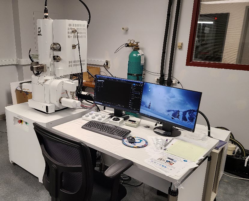
Professor Scott Kirkpatric, JEOL Field Service Engineer Matthew Foil, and Roger Sladek with the newly-installed Field Emission SEM
From the Oakley Observatory to the
MiNDS lab in the Physics and Optical Engineering Department, there was a great deal of excitement at the beginning of the 2020-2021 academic year. A new SEM was being installed at Rose-Hulman Institute of Technology in Terre Haute, Indiana. It prompted the astronomy professor to post a photo on the department’s Facebook page with the comment, “At the Oakley Observatory, we typically look at things that are very large and very far away, but Rose-Hulman's Physics and Optical Engineering department also looks at the very small! The department is currently installing our new Scanning Electron Microscope! We look forward to sharing some small-scale images with you all soon from our new instrument!”
The new Field Emission SEM at Rose-Hulman, one of the highest-ranked STEM schools in the USA, replaces a 21-year-old microscope that had been upgraded extensively, but “We had worked ourselves technology and IT-wise right out of the machine,” says Roger Sladek, Technician/Machinist for the Department of Physics and Optical Engineering.
Roger and Prof. Scott Kirkpatrick, Director for Micro Nano Devices and Systems (MiNDS) and Associate Professor of Physics and Optical Engineering, traveled to JEOL USA headquarters in Peabody, Massachusetts to see a demo of a new JSM-F100 Field Emission SEM. Though not formally trained on SEM, Roger has always had a natural aptitude for machines of all kinds and was an Aerospace CNC machinist before managing all the lab equipment in the department. The demo of the new instrument opened his eyes to how technology has improved, and he appreciated having his questions answered thoroughly so he could learn even more about the capabilities.
Live EDS analysis is possible with the new SEM
“We chose the equipment based on the quality of manufacturing, software control, and ease of use. I also liked that we could restrict some parameters from the students.” He had found in earlier classes that, “Most seemed to think more current and voltage made the image better, which meant I had to replace the filament all the time!”
He adds, “One of the great things about Rose-Hulman is we allow undergraduates to utilize equipment that normally only graduate level students would use.” Students first learn to use the SEM and then apply it to analysis of CNT’s in their Nanotech 2 class. Freshmen get an introduction to SEM in Intro to Nanoengineering. And in the Semiconductors 3 and MEMS 2, students utilize any tool they need. “A graduate course in optics will also utilize the SEM to create various patterns for photonics. We have a few mechanical classes such as ‘material failure’ that also may utilize the SEM for observing fracture surfaces,” Scott adds.
Images courtesy of MiNDS Lab, Rose-Hulman Institute of Technology
The PhOE department offers three degrees: Physics, Engineering Physics, and Optical Engineering with a multitude of Minors and certificates including Astronomy, Semiconductors, Solid State, and Optics.
The ratio of faculty to students is small enough that there is ample time with the professors. Equipment use is under Roger’s guidance, and he handles scheduling of the instruments while grabbing windows of opportunity for preventive maintenance. Meanwhile he continues to learn new things himself. During the installation he was working closely with the JEOL Field Service engineer, Matthew Foil, and was also installing and learning about the JB Nabity Nanometer Pattern Generation System (NPGS) for electron beam and ion beam lithography that will be done with the SEM.
The SEM will be also be used to look at biologicals for the Biology and Biomedical Engineering Department and Roger adds, “I want to add a tabletop plasma cleaner before then, because hydrocarbons will contaminate the sample and the chamber.” Students will learn proper sample preparation before putting things into the SEM like biological samples and tissues. Then there are the Chemical Engineering students who will use the SEM’s EDS (Energy-Dispersive Spectroscopy) to characterize different elements - “New and exciting levels of science to me,” says Roger.
With COVID protocols limiting the number of people allowed in the lab at one time, classes are hybrid. “This year we are keeping our contact low and distances large. Students hold lab with a remote partner. More information, lectures, etc. had been moving online prior to COVID; this just accelerated the process,” Scott explains.
Roger continues, “Normally, the Professor goes through loading samples, pulling an image, and teaching how SEM works all the way down from the emitter to the sample so they understand what’s actually going on in the column. We want them to understand this is how we’re creating the image, how if the edges are bright white the contrast is bad and a charge is building, they have to ground the sample better.” The goal is to give students the knowledge they need to figure out what to do for themselves, not just giving them the answer. The small private institution continues to provide a top-notch education with graduates that are business ready. “Versus someone who’s done nothing but see the machine and a technician prepare their sample for them got their images, and then moved on. We allow them to do what they need to do but not anything that will jeopardize the machine. They’ll understand the difference between imaging at 2, 10, 20, 30kV and the difference in working distances from 40mm to 2mm,” says Roger.
As for the astronomy professor’s interest in SEM, Scott says, “Physics of the large and very small are always intersecting. C60 (buckyballs) was first discovered as an absorption line in space before being realized as an interesting material. He is most welcome to use the SEM, and I have on occasion played with telescopes, and helped fit light curves to asteroids.”