Northwestern University Atomic and Nanoscale Characterization (NUANCE) Center
Center of Excellence for JEOL
Just as the surge in nanotechnology research began,
Northwestern University Atomic and Nanoscale Characterization (NUANCE) Center launched in 2001-2002 as a resource to academia and industry in the Chicago area. Under the direction of Prof. Vinayak Dravid, the center has since become the largest microscopy and surface science resource throughout the region.
One of five NUANCE facilities, the Electron Probe Instrumentation Center (EPIC) houses one of the most complete arsenals of state-of-the-art electron microscopes in the world, and now also serves as a Center of Excellence for JEOL.
SEM Laboratory Manager Tirzah Abbott described NUANCE, explaining that, “We are part of the
SHyNE Resource (Soft and Hybrid Nanotechnology Experimental Resource), a coordinated infrastructure funded by NSF (National Science Foundation).” It serves scientists and engineers from industry, academia, government, and non-profit sectors as part of the NSF National Nanotechnology Coordinated Infrastructure (NNCI) program.”
Tirzah joined NUANCE in 2016 with extensive experience in SEM and a Master’s degree in Geology, specializing in stable isotope geochemistry. She manages the SEM facility where she trains new users of the microscopes and helps develop their applications. She is also involved in teaching and outreach and enjoys developing out-of-the-box SEM techniques and applications. Recently, Tirzah has specialized in use of the
JEOL JSM-7900F Field Emission SEM.
All training was done online during this past year after a brief closure at the onset of the pandemic. Tirzah was instrumental in developing the infrastructure, protocols, and content to enable these effective training capabilities. Now it is the norm that training and technical assistance is done remotely, and operations are in full swing on-site while observing social distancing. “That’s been working out very well,” she says, especially with upgrades to enhance the remote learning experience. “Now we have the capability to share multiple screens online all at once and can record all the training and meetings for future reference.”
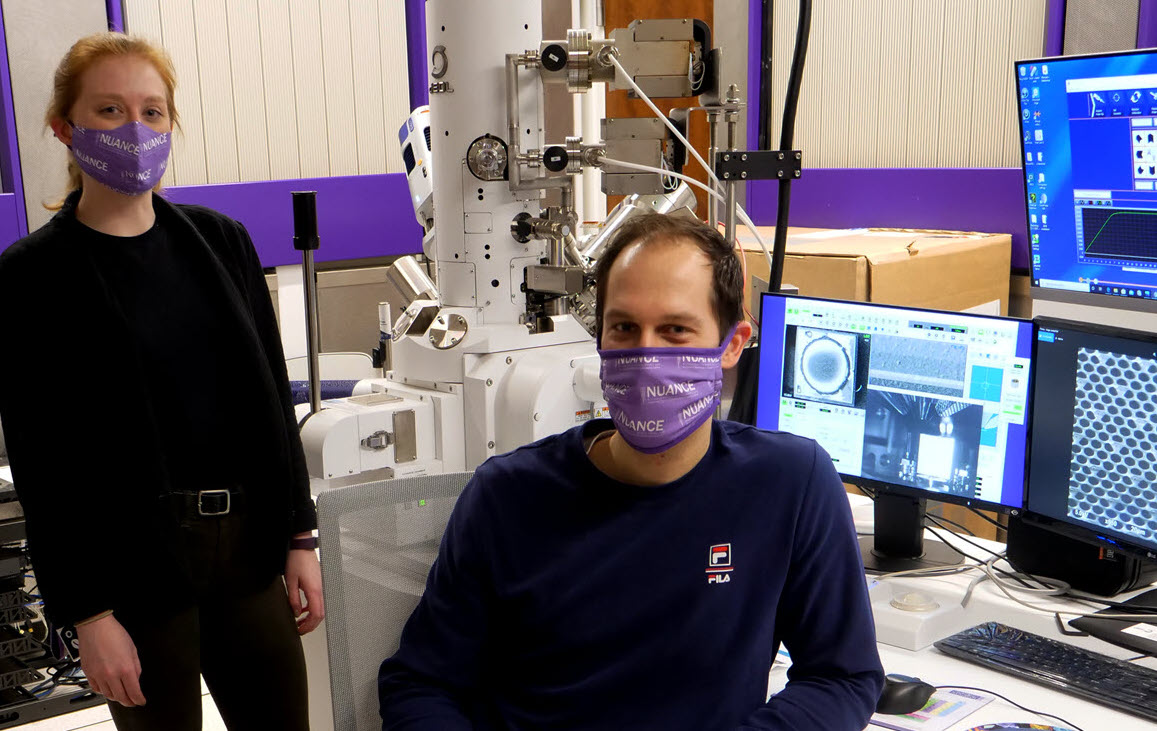
Tirzah and Facility Manager FIB&TEM/Research Associate Paul Smeets have been directly involved in installing and commissioning the new
JEOL JIB-4700F dual-beam FIB-SEM and work together to train users and help clients with their microscopy work. The Multibeam system is used for (automated) TEM and atom probe tomography (APT) sample preparation, and is optimized for applications including three-dimensional (3D) tomography, 3D EBSD, and 3D EDS analysis, therefore bringing all-new capabilities to the NUANCE Center.
Paul spoke to us from the new
JEM-ARM300F room where he was working to image and analyze materials at the atomic level. He has been at NUANCE since 2019, after joining Northwestern University in 2016 as a Postdoctoral Research Fellow. His primary focus has been on characterization of soft-hard matter interfaces in materials, predominantly in teeth and other (bio)minerals. “There are lots of different materials that I work on as well as trying to do some of my own projects, such as characterization of human enamel crystallites using 4D STEM experiments, in order to elucidate structural details which can lead to tooth decay. I use the FIB-SEM to prepare the samples and visualize these in the ARM300F, which is rather intricate given the sensitivity of the material to high energy electrons. Now that we have capable direct electron detectors and the possibility to explore lower accelerating voltages down to 40kV on the ARM300, I am excited to explore this further,” Paul said.
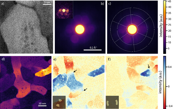
a) Cryo-STEM image displaying part of an enamel crystallite (see Pauls’ recently first co-authored Nature paper) b) Average diffraction pattern of the 4D STEM data set (high SNR). Inset: single diffraction pattern of the 4D STEM data set (low SNR). c) Average diffraction pattern with 12 segmented virtual detectors (indicated by white lines). d) Virtual image created from the average diffraction pattern, combining intensities from all segmented virtual detectors. e,f) Maps displaying the differences in intensity between two selected opposite partial virtual detectors (indicated in inset). This difference in intensity is indicated in the red to blue color bar on the right. The black arrows indicate places within single grains that show variations in intensity between the opposed virtual detectors, which signify a tilt in the crystallographic directions of the apatite lattice with respect to one other. A special thanks to Dr. Roberto dos Reis & Stephanie M. Ribet for helping with data analysis using Python scripting.
Both Paul and Tirzah are kept busy using SEM, FIB-SEM, and TEM to help clients with samples ranging from botany and microfossils to high-profile artwork and advanced semiconductors. They have also collaborated on research and papers with a variety of research groups. They coordinate outreach programs and give or arrange for
Tech Talks, such as a recent Tech Talk on the
JEOL 7900FLV Field Emission SEM,
FIB-SEM, and the
Workshop on 4D STEM. They participate in an annual
NUANCE Fest on
National Nano Day and hold a SEM and TEM image contest. In December 2020, Tirzah won the
JEOL Image Contest with her SEM Image “Little Rock Candy Mountains” (calcite crystals precipitated on the surface of a fossil radiolarian).