JEOL USA Press Releases

JEOL's JAM-5200EBM, the large-format electron-beam powder bed fusion system used to print the full-size tungsten tiles.

NC State, Oak Ridge National Laboratory and JEOL put full-size 3D-printed tungsten tiles into a U.S. fusion facility

RALEIGH, N.C. (October 22, 2026): A team from North Carolina State University, Oak Ridge National Laboratory (ORNL) and JEOL Ltd. has 3D printed full-size tungsten tiles for the inside wall of a fusion device, finished them to tight tolerances and tested them in the DIII-D National Fusion Facility in San Diego. The tile surfaces were directly exposed to 74 plasma discharges with significant heat and particle flux, and came through intact.

The project went from invitation to installed hardware in about eight months. It came out of NC State's research partnership with DIII-D National Fusion Facility and brought together three groups with deep expertise in electron-beam powder bed fusion (EB-PBF) and tungsten additive manufacturing. For this project, JEOL's large-format EB-PBF system and engineering team in Japan made printing the tiles at full size possible, ORNL contributed fusion materials expertise and funding, and NC State led the finishing and characterization.

"When DIII-D asked if we could do this, I said yes without blinking and then figured we'd have to sort out the details," said Dr. Tim Horn, Associate Professor of mechanical and aerospace engineering and research director at the Center for Additive Manufacturing and Logistics (CAMAL) at NC State. "Our 'Think and Do' motto aside, in reality, there were major challenges to making this happen. We understood the processing science behind tungsten additive manufacturing and the physics of scaling up. What we needed was the hardware and partners who could move fast. ORNL and JEOL were exactly that."
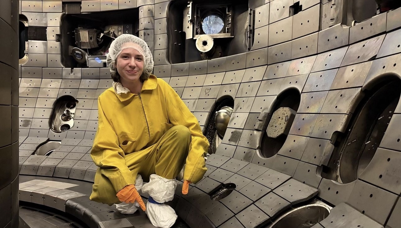
NC State nuclear engineering undergraduate Olivia Mehalick inside the DIII-D vacuum vessel during installation of the 3D-printed tungsten tiles.

Why tungsten, and why it's hard

In a fusion tokamak like DIII-D, the core plasma temperature reaches well over 100 million °C. Much of its exhaust heat lands on the divertor, a region at the bottom of the machine lined with protective tiles. In ITER and future power plants, those tiles must handle steady heat loads of 10 to 20 megawatts per square meter, more than 10,000 times the intensity of direct sunlight on a summer day, with brief bursts far higher. That means the tile material has to do several jobs at once: survive extreme heat and constant bombardment by plasma particles and high-energy neutrons, and conduct heat well enough to carry that load away.

Tungsten is considered a leading material for the job. It has the highest melting point of any metal, 3,422 °C (6,192 °F), more than twice that of steel. It is also dense: at 19.3 grams per cubic centimeter, it weighs about 2.4 times as much as steel for the same size, roughly as much as gold. For comparison, a bowling ball made of tungsten would weigh more than 100 kilograms (~225 lbs), about 14 times as much as a regulation ball. 

The problem with making tungsten parts is the ductile-to-brittle transition temperature (DBTT). Below roughly 200 to 600 °C, tungsten cracks rather than bends, behaving more like glass than metal. That makes it very hard to manufacture with traditional machining or joining processes, and the high melting temperature rules out most casting and forming processes, so there is a significant amount of research effort focused on additive manufacturing, or 3D printing, approaches. However, most attempts to 3D print tungsten, nearly all using lasers as the heat source for printing, have ended up porous and riddled with cracks.

Several years ago, ORNL and NC State pioneered a different approach: electron-beam powder bed fusion (EB-PBF). An electron beam melts tungsten powder layer by layer in a vacuum chamber while the fast scanning capability of an electron beam keeps the surrounding material hot and held above 1,400 °C, well above the brittle range. The partners produced dense, crack-free tungsten this way and published the results in 2021 in the Journal of Nuclear Materials. That work helped lead to a joint ARPA-E / DOE Fusion Energy Sciences program on tungsten under ARPA-E's GAMOW initiative where Dr. Michael Kirka and Dr. Chris Ledford at ORNL led further developments on EB-PBF of tungsten.

"Tungsten is currently the material everyone wants in a fusion reactor, but it is extremely difficult to manufacture into complex shapes," Kirka said. "We were able to do this with electron-beam additive manufacturing, when most of the field thought printed tungsten would always crack. These tiles are the payoff from years of that work."

How the collaboration came together

NC State and DIII-D already work closely on the plasma physics side. Dr. Florian Laggner, an assistant professor and plasma physicist in NC State's Department of Nuclear Engineering, leads a collaboration with DIII-D's neutral beam team to develop new radio-frequency ion sources for the beams that heat the facility's plasma. His group is now assembling a 200-kilowatt prototype source at NC State.

The tile project grew out of the materials side of that relationship, where plasma physics meets advanced manufacturing. NC State joined the DIII-D program as a participating organization to enable university researchers to more rapidly advance their work using internal funds. This access, led by Laggner and Horn, is allowing them to develop and test new ways to make the materials that line the inside of fusion reactors.

In 2025, that partnership put small buttons of NC State's printed tungsten into DIII-D using the facility's Divertor Materials Evaluation System (DiMES). In tests led by NC State nuclear engineering Ph.D. student Aaliyah Zuniga, the samples saw heat fluxes near 20 megawatts per square meter, with brief peaks above 35, and showed minimal surface damage.

Those results earned an invitation. In December 2025, Dr. Jonathan Coburn of Sandia National Laboratories, who led the novel tile portion of DIII-D's 2026 Tungsten Tile Testing campaign, asked the NC State team to test a full-size printed tile.

"The AM tungsten performed quite well during Aaliyah's DiMES testing, so there was both motivation and confidence for producing a larger component for further testing," Coburn said.

The catch was scale. The DIII-D tile for this effort measures about 140 by 130 millimeters, and the largest tungsten part NC State had printed was about 50 millimeters across. It was clear that NC State's own machines could not hold such a high-temperature material at the required conditions over a build that large.

Haozhi Zhang, a postdoctoral researcher in Horn's lab who works on electron-beam printing of tungsten, looked into what it would take to print and finish a part that large, from new scan strategies to keeping a much bigger build area hot enough while it melts. "Testing an additively manufactured, full-size tungsten tile at DIII-D would be a first-of-its-kind achievement in the field," Zhang said.

Scaling up with JEOL

That is where JEOL came in. At the time, JEOL was already partnering with ORNL on additive manufacturing and placing one of its systems at the laboratory, and had recently begun developing tungsten printing independently on its own systems. And when the DIII-D invitation arrived, Horn happened to be in Japan visiting JEOL to discuss tungsten printing. It quickly became clear that JEOL's large-format EB-PBF system, the JAM-5200EBM, with its open control system, and JEOL's expertise could build the full-size tiles.

JEOL is, perhaps, best known worldwide for its scanning and transmission electron microscopes, but the company also has a long history in electron beam welding and electron beam lithography. Building a metal 3D printer around a precisely steered electron beam was a logical evolution, and the JAM-5200EBM draws on decades of JEOL's experience designing and building precision electron beam systems.
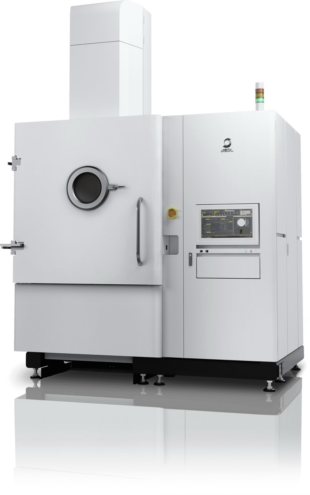
JEOL's JAM-5200EBM, the large-format electron-beam powder bed fusion system used to print the full-size tungsten tiles. Image: JEOL

In early 2026, with the DIII-D proposal accepted, Horn and Laggner brought together Zane Marek and Jonathan Buckley of JEOL USA and Michael Kirka and Christopher Ledford of ORNL. JEOL engineers Satoshi Ono and Akimine Hatsuda printed the tiles at JEOL's facility in Akishima, Japan, with Zane Marek and Jonathan Buckley of JEOL USA serving as the project's main points of contact from JEOL. ORNL's Fusion Materials Core Program, with Michael Kirka leading ORNL's role and the support of Yutai Kato, director of ORNL's Materials Science and Technology Division, funded the fabrication.

Working with ORNL and NC State, the JEOL team turned the tile design into a working build. They set the support structure and electron-beam parameters for the full-size parts, then printed several iterations of the flat and domed designs, refining the build after the first run to improve dimensional accuracy. The final as-printed tiles had no major defects and met all design tolerances in every dimension.

 "We appreciate the opportunity to collaborate with NC State, ORNL, and General Atomics, on a project that brings together advanced materials research, fusion science, and JEOL's long-standing expertise in precisely controlled electron-beam technologies," said Tom Isabell, President of JEOL USA. "Producing full-size tungsten tiles for DIII-D is exactly the kind of challenge our JAM-5200EBM system was designed to address. By applying our optics, beam-control, and additive manufacturing expertise alongside outstanding partners, we are helping demonstrate a practical path toward the complex, high-performance components future fusion systems will require.”  The partnership is now growing. JEOL has a system at ORNL and is in the process of placing an EB-PBF system at NC State to further strengthen the three-way collaboration among NC State, JEOL and ORNL on tungsten and other fusion materials.

"This is what a good partnership looks like," Horn said. "Every partner brought something to the table." NC State co-developed the electron-beam tungsten process, wrote the proposal, finished the tiles and is leading their analysis. ORNL funded the fabrication through its Fusion Materials Core Program and, building off its own tungsten printing development, helped scale up the print. JEOL engineers used the company's large-format EB-PBF system and printed several iterations of flat and domed tile designs. And the DIII-D team, including Sandia National Laboratories, Princeton Plasma Physics Laboratory and General Atomics, which operates DIII-D for the US Department of Energy, ran the design reviews, installation and experiments. "None of us could have done it alone," Horn said. 

"Fusion has been called the energy source of the future for a long time. One of the things holding it back is materials that can survive inside the machine," Kirka said. "Showing that printed tungsten tiles can go into a working tokamak and come out intact moves additive manufacturing from 'promising' to 'proven' for fusion."

From printer to plasma

Each tile pair measures about 136 by 143 millimeters and 20 millimeters thick.

Back at NC State, Zhang and nuclear engineering undergraduate Olivia Mehalick carried out the finishing. Mehalick used wire electrical discharge machining (EDM), which cuts with an electrically charged wire and puts no mechanical stress on the brittle tungsten, to shape the mounting features and a gently domed surface with a radius of about 1 meter. A multi-axis CNC grinder, programmed with a digital twin of the tile, then removed about 250 microns from the plasma-facing surface. The finished tiles had mirror-like surfaces and met DIII-D's tolerances.
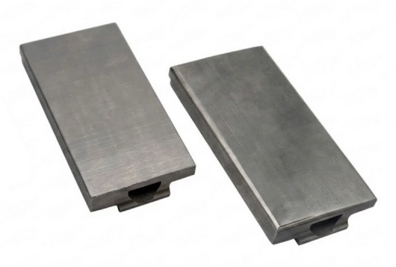
Finished flat and domed tungsten tiles with mirror-like plasma-facing surfaces, ready for installation in DIII-D. 

The tiles were mounted on copper-alloy pedestals and installed in DIII-D's lower divertor in July 2026. Mehalick traveled to San Diego for the installation and participated in the experiments.

Over the course DIII-D’s Tile Testing Campaign, the AM tiles saw 3 days of direct plasma exposure. 74 of these plasma discharges were in high-confinement "H-mode" at medium-to-high power, for about four minutes of total plasma exposure.

"As far as we could tell in the control room, your AM tiles performed really well," Coburn told the team after the campaign.

A neighboring conventional tile that was slightly out of alignment melted along its leading edge and spattered onto one of the printed tiles, giving the team an unplanned look at how the printed material responds.

The divertor shelf before plasma exposure, with the printed flat split tile pair at center. [Photo credit: Ryan Hood, SNL]

After exposure: the printed tiles survived intact. Marks from the misaligned neighboring tile's melted edge are visible nearby. [Photo credit: Ryan Hood, SNL]

The tiles are now being removed, imaged and surface-scanned to compare with their condition before exposure. After a radiation survey, they will return to NC State for detailed analysis.

The project was presented at the AM2F 2026, the Additive Manufacturing and Advanced Materials in Fusion conference (https://am2f2026.psfc.mit.edu/) in Cambridge, Mass., on Aug. 31. In September, printed tungsten tiles from the project were on display at JEOL's booth at IMTS 2026, the International Manufacturing Technology Show, in Chicago.

"Fusion is moving fast. Qualifying new materials and manufacturing methods requires fusion-relevant data," Laggner said. "By exposing additively manufactured tungsten in DIII-D, we are generating that data on survivability and erosion."

"DIII-D lets us put candidate materials in front of a real fusion plasma and see what happens," Dr. Chris Ledford from ORNL said. "Seeing additively manufactured tungsten go from small test buttons to full-size tiles in the divertor in less than a year is remarkable, and the data from this campaign will help guide how tungsten components are designed for ITER and beyond."

Students at the center

"Our students and Post-docs drove this effort home," Horn said. "Aaliyah's earlier plasma tests are the reason DIII-D asked us in the first place. Olivia, an undergraduate, took these tiles from rough prints to finished parts sitting in a national fusion facility, then participated in the control room while they were tested. That's an experience most students never get."

Mehalick and Zuniga both study fusion from the plasma physics side, Mehalick as an undergraduate and Zuniga as a Ph.D. student in nuclear engineering. Neither came in as a manufacturing specialist. Both took the initiative to learn to run the wire EDM, grinding and characterization equipment at CAMAL, with training from Zhang, so they could see the project through themselves.

"In my classes, the wall of a fusion reactor is a boundary condition in an equation," Mehalick said. "This project made it a real part I had to cut, grind and measure. Learning to run the manufacturing equipment at CAMAL, and then monitoring these tiles during the plasma exposure with cameras from the DIII-D control room, changed how I think about what it takes to actually build a fusion machine." 

"Our first DiMES samples would fit on a fingertip, so seeing that work lead to full-size tiles in the same machine less than a year later has been amazing," said Zuniga, who interned at ORNL this summer. "Spending the summer at Oak Ridge also showed me how much universities, national labs and industry depend on each other to move fusion materials forward." 

The team

Name

Organization

Tim Horn NC State, Mechanical and Aerospace Engineering; CAMAL
Florian Laggner NC State, Nuclear Engineering
Haozhi Zhang NC State, Mechanical and Aerospace Engineering (postdoctoral researcher)
Aaliyah Zuniga (Ph.D. student) NC State, Nuclear Engineering
Olivia Mehalick (undergraduate) NC State, Nuclear Engineering
Yutai Kato Oak Ridge National Laboratory
Michael Kirka Oak Ridge National Laboratory
Christopher Ledford Oak Ridge National Laboratory
Ezekial Unterberg Oak Ridge National Laboratory
Zane Marek JEOL USA, Inc.
Jonathan Buckley JEOL USA, Inc.
Satoshi Ono JEOL Ltd., Japan
Akimine Hatsuda JEOL Ltd., Japan
Jonathan Coburn Sandia National Laboratories
Florian Effenberg Princeton Plasma Physics Laboratory
Tyler Abrams General Atomics / DIII-D
Karl Schultz General Atomics / DIII-D
Kyle Teixeira General Atomics / DIII-D

Funding

This material is based upon work supported by the U.S. Department of Energy, Office of Science, Office of Fusion Energy Sciences, using the DIII-D National Fusion Facility, a DOE Office of Science user facility, under contracts DE-FC02-04ER54698, DE-AC05-00OR22725 with UT-Battelle LLC, DE-NA0003525 with NTESS under DOE NNSA, and DE-AC02-09CH11466. Tile fabrication was funded by ORNL's Fusion Materials Core Program.

Disclaimer

Disclaimer: This report was prepared as an account of work sponsored by an agency of the United States Government. Neither the United States Government nor any agency thereof, nor any of their employees, makes any warranty, express or implied, or assumes any legal liability or responsibility for the accuracy, completeness, or usefulness of any information, apparatus, product, or process disclosed, or represents that its use would not infringe privately owned rights. Reference herein to any specific commercial product, process, or service by trade name, trademark, manufacturer, or otherwise does not necessarily constitute or imply its endorsement, recommendation, or favoring by the United States Government or any agency thereof. The views and opinions of authors expressed herein do not necessarily state or reflect those of the United States Government or any agency thereof.

JCM-7000Plus NeoScope™

Launch of the New Benchtop Scanning Electron Microscope “JCM-7000Plus NeoScope™”

JEOL Ltd. (President & CEO: Izumi Oi) has developed the benchtop scanning electron microscope (SEM) “JCM-7000Plus” and will begin sales on September 1, 2026.

Development Background

Benchtop scanning electron microscopes are increasingly used across a wide range of fields, including electrical and electronics, automotive and machinery, steel and metals, chemical and pharmaceuticals. They are utilized not only in research and development but also in manufacturing-related applications, such as quality control and product inspection. In addition, they are also adopted in educational settings at middle and high schools as well as universities. Given the diverse range of applications, there is growing demand for improved operational efficiency, simpler and more automated operation, and enhanced observation, analysis, and measurement performance.

To meet these needs, on the hardware side, we have first expanded the landing voltage (accelerating voltage) to 20kV. This has improved resolution to 6nm, enabling measurements at higher magnification and with high resolution. 

On the software side, the new JCM-7000Plus retains the simple, user-friendly GUI of the current JCM-7000, including Zeromag, which enables a seamless transition from optical imaging to SEM observation, and the Live Analysis function, which allows real-time elemental analysis during observation. It also adds the enhanced automation feature Neo Action.

In addition to the three existing Live functions (Live Analysis, Live Map, and Live 3D), we have added two new features: Live Particle, which automatically measures particle size and count in real time while observing, and Live Report, which automatically acquires data and generates reports while moving the field of view, a feature available in high-end FE-SEMs. These features simplify routine tasks, making them more intuitive and efficient while significantly supporting users' analytical workflows.

Main Features

  • Expanding landing voltage to 20 kV for improved resolution (secondary electron image: 6 nm, backscattered electron image: 8 nm)

  • Improved backscattered electron detector for enhanced image quality

  • New Live Particle function automatically measures particle size and count, simplifying workflow.

  • Simple and user-friendly GUI retained, with added automation functions for more intuitive and easier operation

ACE eye™ TEM for Semiconductor Analysis

Launch of the ACE eye™ TEM for Semiconductor Analysis

JEOL Ltd. (President & CEO: Izumi Oi) has developed the ACE eye™, a transmission electron microscope (TEM) for semiconductor analysis, and began sales in July 2026.
By automating the entire measurement workflow —from TEM/STEM observation to EDS analysis— the ACE eye™ delivers highly reproducible measurements that are less dependent on operator expertise. It also supports long-duration, continuous automated measurement, helping to improve the efficiency of semiconductor device R&D, process evaluation, and failure analysis.

Background to Development

Semiconductor devices are becoming smaller, more highly integrated, and increasingly three-dimensional. As a result, advanced devices such as gate-all-around (GAA) transistors and 3D NAND are becoming more structurally complex and incorporating a wider variety of materials. In the R&D, process evaluation, and failure analysis of these devices, it is essential not only to observe fine structures and material interfaces at high resolution but also to accurately determine elemental distributions at the nanometer scale.

High-resolution TEM/STEM observation and EDS analysis, however, require the appropriate adjustment of focus, astigmatism, specimen height, beam position, crystal orientation, and other parameters. Consequently, the quality of measurement results and the time required for operation can depend heavily on the operator's level of expertise. In addition, as the number of measurements increases, there is growing demand for more efficient measurement workflows and for continuous automated measurement over extended periods.

To address these challenges and needs, JEOL developed the ACE eye™ TEM for semiconductor analysis. By automating the entire measurement workflow —from TEM/STEM observation to EDS analysis— the instrument delivers highly reproducible measurements that are less dependent on the operator’s level of expertise. It also provides a flexible automation tailored to the measurement objective and operating environment.

The ACE eye™ promotes a shift from operations that require constant decision-making to measurements that users can confidently leave to the instrument. This helps to improve the efficiency of semiconductor device R&D, process evaluation, and failure analysis.

Key Features

  1. Automation

    Measurement conditions and procedures can be configured as recipes, allowing the entire workflow from TEM/STEM observation through EDS analysis to be automated, with operations ranging from semi-automatic to fully automatic according to the intended purpose. The system is equipped as standard with an ASCOR spherical aberration corrector manufactured by CEOS. AI-based automatic aberration correction and advanced automation algorithms improve measurement consistency and reproducibility. In addition, when the system is combined with a large-capacity liquid nitrogen tank, Automation Center automated measurement software (optional), and the MultiSPECPORTER (MSP; optional), long-duration, unattended, continuous automated measurement is possible under specified conditions. The MSP is an autoloading system that stores up to 12 specimen grids under vacuum. Through GUI operation, it automatically inserts each specimen into the microscope column for observation and removes it after observation. Unattended data acquisition in conjunction with Automation Center contributes to the high-throughput operation of the ACE eye™. The MSP also employs a replaceable cartridge system. By reducing the specimen-holder drift associated with the specimen exchange, this system supports high-precision, stable analysis.

  2. Analytical Performance and Reliability

    The combination of a wide-gap pole piece and ASCOR enables both high-resolution observation and high-sensitivity EDS analysis while delivering high magnification reproducibility of ±0.5% in both TEM and STEM modes. The EDS system provides a large solid angle of 2.2 sr when the MSP is not installed, enabling high detection sensitivity. In addition, the high take-off angle reduces shadowing by the specimen and holder. It also enables the acquisition of clean spectra with suppressed system peaks, thereby supporting reliable elemental analysis. Measurement reproducibility and reliability are further enhanced using LogChecker (optional), which monitors instrument status and the external environment, and by a column enclosure that suppresses external disturbances.

  3. Operability

    The intuitive TEM Center user interface enables observation and measurement through simple mouse operations. In Automation Center, Operator and Administrator modes enable configuration and management according to each user’s role. Seamless integration with Gatan cameras (optional; some camera models are not supported) provides a smooth workflow from image acquisition to data storage. In addition, a newly developed holder enables one-touch installation of specimen grids. Combined with TEM-FIB linkage using a TEM-FIB dual-axis tilt linkage cartridge and a dedicated TEM holder (both optional), it reduces the operator's workload and minimizes specimen-handling risks.

Designed as the “eye” of advanced semiconductor analysis, the ACE eye™ rapidly delivers reliable structural and compositional information.

Main Specifications

ACE eye™ High Throughput Analytical Electron Microscope

TEM resolution
(at 200 kV)
Particle image: ≤0.27 nm
Lattice image: ≤0.10 nm
Information limit: ≤0.14 nm
STEM resolution
(at 200 kV)
Dark-field STEM image: ≤0.10 nm
Bright-field STEM image: ≤0.10 nm
Electron gun Cold field-emission electron gun (CFEG)
Accelerating voltage 60 to 200 kV
(Standard: 200 kV and 80 kV; other accelerating voltages are optional.)
Aberration corrector STEM: ASCOR (standard configuration)
Options JEOL 160 mm2 SDD (Dual), Automation Center, MultiSPECPORTER, Tomography, EELS
Note: All performance values are based on measurement conditions specified by JEOL.
Sales Launch of the CRYO ARM™ 300S and CRYO ARM™ 200S

Sales Launch of the CRYO ARM™ 300S and CRYO ARM™ 200S : one cryo-electron microscope for single-particle analysis, cryo-electron tomography and 3DED/MicroED

Tokyo, Japan — 3rd August 2026— JEOL Ltd. (President & CEO: Izumi Oi) today announced the CRYO ARM™ 300S and CRYO ARM™ 200S, JEOL’s latest 300 kV and 200kV cold field-emission cryo-electron microscope that offers single-particle analysis (SPA), cryo-electron tomography (cryo-ET), 3DED/MicroED and beyond, all in one highly automated instrument. The CRYO ARM™ 300S and 200S are engineered to deliver high-resolution structural data with the stability, throughput and ease of use that today’s structural-biology and drug-discovery laboratories require.

Cryo-EM has become central to structural biology and structure-based drug design, yet everyday productivity is often limited by instrument downtime, complex setup and the scarcity of expert operators. The CRYO ARM™ 300S and 200S address these constraints directly — combining hardware refinements with AI-based automated data acquisition so laboratories can collect more high-quality data per day, with less hands-on expertise and more consistent results.

Main Features

From “human selection” to “AI selection”: automated acquisition with SmartScope multigrid

Even with modern microscopes, cryo-EM data collection often still depends on an experienced user setting up each grid one by one, then choosing the right grid squares and holes before imaging can begin. That takes time, ties up expert staff, and limits how much data a lab can collect.

The CRYO ARM™ 300S and 200S integrates open-source AI driven software, SmartScope※ multigrid to remove that bottleneck. Instead of requiring an expert to guide each grid manually, the system can work more autonomously across multiple grids: identifying grid squares, selecting holes for imaging, and moving into data collection with minimal operator input. The result is a real shift from semi-automated to automated cryo-EM data collection. More users can run sessions, expert time is freed up, and labs can collect more data from every microscope run.

※Jonathan Bouvette et al., eLife, 11:e80047 (2022)

Higher throughput and longer autonomous runs

Fringe-free illumination expands the usable imaging area to improve acquisition efficiency, reaching approximately 1,000 images per hour in practical operation. Simultaneously specimen exchange capacity increase from four to six cartridges, cuts the frequency and duration of sample exchanges while further extending the unattended data-collection runs — so more of each day is spent acquiring data.

Seamless, reproducible cryo-CLEM with CryoLameller integration

Frozen specimens on the CRYO ARM™ cartridge can start its journey in CryoLameller (cryo-FIB-SEM) for lamella preparation, with positional information preserved end to end, before moving to the TEM. Because the CryoLameller is fitted with an in-situ fluorescence microscope, users gain a continuous, reproducible cryo-CLEM workflow spanning targeting, milling and imaging — well suited to in-situ cellular tomography.

Designed for real-world reliability

Beyond raw capability, the CRYO ARM™ 300S and 200S were re-engineered for the more stability, straighter workflow and further reliability that R&D and service environments depend on — so advanced observation and dependable daily operation are delivered by the same instrument.

Main specifications

Electron gun Cold field-emission electron gun
Standard accelerating voltage CRYO ARM™ 300S (300 kV)
CRYO ARM™ 200S (200 kV)
Energy filter In-column Omega filter
Maximum specimen tilt ±70°
Specimen storage (autoloader) Up to 12 specimens
JEOL USA Announces Expansion of Board of Directors and Leadership Appointments

JEOL USA Announces Expansion of Board of Directors and Leadership Appointments

July 16, 2026 — Peabody, Mass. — JEOL USA, Inc. has expanded its Board of Directors with the appointment of two members of its leadership team, Donna Gosselin and Steve Tryon. In addition, Dr. Thomas Isabell was appointed President of JEOL USA. Together, they bring decades of leadership experience spanning product management, applications, and field service, further strengthening the company's governance and strategic direction.

Dr. Thomas Isabell has been a member of the JEOL management team since 2003, serving most recently as Vice President of Sales and Marketing and, before that, as Vice President of Product Management. He has been instrumental in the introduction of the company's ARM series and CryoARM transmission electron microscopes. Dr. Isabell holds a Ph.D. in Materials Science and Engineering from Northwestern University and a B.S. in the same field from the University of Minnesota.

Donna Gosselin is Director of Product Management and a chemist with more than 20 years of experience in scanning electron microscopy and energy dispersive X-ray spectroscopy. She joined the JEOL USA electron microscopy product team in 2002, following more than 15 years as an analytical and research chemist in industry. Her combined technical and industry background helps align customer needs with product innovation.

Steve Tryon is Director and General Manager of the Service Division. He began his career with JEOL USA in 1995 as a Field Service Engineer in Southern California and moved through field service and service management roles over three decades, relocating to the corporate headquarters in Peabody, Massachusetts in 2016. He holds degrees in Engineering Technology and Business, along with credentials in Supervisory Management and Field Service Management.


Sales Launch of the Laser SEM System “LazEdge”

Sales Launch of the Laser SEM System “LazEdge”

JEOL Ltd. (President & CEO: Izumi Oi) has developed the “LazEdge”, an SEM system equipped with a laser processing system, and begins sales on May 25, 2026. Cross-section preparation instruments such as the focused ion beam system (FIB system), are widely used in science and technology fields across research institutes, universities, and industries. In recent years, demand is increasing for a system that can process large-areas at a high speed, while achieving high-quality of the processed surface. “LazEdge” is an instrument integrating JEOL’s SEM with the laser technology proprietary of Hamamatsu Photonics K.K., and enables laser processing inside the specimen chamber of the electron microscope.

This system enables high-quality cross-section specimens produced through high-speed, large-area processing to be transferred seamlessly to subsequent analyses, such as SEM observation, elemental analysis, and crystal orientation analysis, without exposure to the external environment. As a result, it meets a wide range of analytical needs, including metal specimen analysis, battery analysis requiring air-isolation, and semiconductor failure analysis requiring high-speed cross-sectioning.

Main Features

High-quality cross-sectioning inside the specimen chamber

By integrating a laser processing system into the SEM, LazEdge achieves high-quality cross-sectioning of large-areas with reduced LIPSS structures at a high speed in the specimen chamber, through the use of a proprietary optical system that enables phase modulation of the laser beam spatially.

Stable and clean processing enabled by “LazEdge Shield”

The proprietary shielding technology “LazEdge Shield”, minimizes debris generated during processing from scattering, and achieves clean processing without the contamination of detectors, columns, and specimen chamber walls. Moreover, the laser system can simultaneously focus on the specimen processing position and the laser irradiation position on the shield. This technology allows for processing and cleaning of the shield (contamination prevention) at the same time. These technologies provide high-quality cross-sectioning while always maintaining stable power.

Seamless, high-throughput processing and observation

By installing a shield inside the SEM specimen chamber and performing the processing within the chamber, it is possible to carry out both processing and observation seamlessly and with high throughput. For example, in EBSD measurements, laser processing alone can produce cross-section with sufficient quality for EBSD measurement. By automatically repeating the processing and measurement, 3D EBSD acquisition is also possible.

Ultra-fast analysis of protein 3D structures ― sample preparation for cryo-EM in 10 minutes

Ultra-fast analysis of protein 3D structures ― sample preparation for cryo-EM in 10 minutes

The 3D structure of a biomolecule, such as a protein is becoming an essential information for research and development of biochemistry and drug discovery. While the analysis method using cryo-EM is widespread, a tool to dramatically improve the speed of analysis work, "EG-grid™" was developed by Prof. Inoue. We interviewed Prof. Inoue about its characteristics.

Rapid Penetration of cryo-EM

As a method for 3D structural analysis of proteins, cryo-electron microscopy (cryo-EM) has rapidly spread. In the international public database PDB (Protein Data Bank), 3D structure data of biomolecules (proteins, nucleic acids, etc.) that are newly elucidated are registered day by day. The data is disclosed once the related paper is released. Among the structural data disclosed, the ones elucidated by electron microscopes reached 5,791 in a year in 2024. This occupies 37% of the total number of disclosed data in that year.

Number of disclosed PDB by analysis method in a year. Created based on statistical data available with PDB. The record in 2025 is as of December 3.

According to the graph, the data using electron microscope began increasing around 2017. This year, the three researchers who developed the fundamental technology of the cryo-electron microscope were awarded the Nobel Prize in Chemistry. "Triggered by the Nobel prize, the awareness of cryo-EM and its method was increased, accelerating the use", says Prof. Tsuyoshi Inoue (Graduate School of Pharmaceutical Science, The University of Osaka).

The reason for the popularity of the cryo-EM is that the crystallization of protein, which used to be an inevitable process in an X-ray crystal structure analysis, is not required. The X-ray crystal structure analysis is a major method for elucidating the 3D structure. However, in this method, protein needs to be made into a large crystal of about 100 μm. Sample preparation takes several months or more. Also, there are proteins and complexes that are hard to crystalize. The cryo-EM can analyze proteins that are hard to crystalize, which is the advantage of the cryo-EM.

Moreover, analysis is possible even if there are only small sample amount available, which is another great advantage. Challenging structure analysis becomes easy even for proteins whose purification is difficult and a complex which is unstable and tends to easily aggregate.

Sample preparation in a month even for the cryo-EM

Then, does cryo-EM require any processing? Yes, it does. In the early stage, sample preparation and taking electron micrographs took some time.

For analysis of a 3D structure, a single-particle analysis method is used. In this method, many images of a discrete single particle, are taken by the cryo-EM. To increase accuracy, many images taken from various angles need to be prepared and they are reconstructed into a 3D structure using a computer. For this purpose, it is necessary to prepare an appropriate sample which allows efficient image acquisition, thereby improving the overall research speed.

For preparing a sample, the ice-embedding method was traditionally used. This is a method to rapidly freeze a solution to embed proteins within amorphous ice. However, this method presented challenges in adjusting the concentration. If the concentration is too high, particles overlap and usable images cannot be obtained. On the other hand, if the concentration is too low, the number of particles decreases, and imaging efficiency is reduced. In addition, if the ice is thick and protein particles are distributed in the thickness direction, the number of particles that can be focused is limited, further reducing imaging efficiency.

Issues in sample preparation by ice-embedding method

"Adjusting concentration is a tough thing. However, the most critical problem in the ice embedding method is the preferred orientation, where the proteins align in the same direction!" (Prof. Inoue)

The preferred orientation is generated during freezing processes. But in some cases, the orientation to the same direction occurs before freezing. These are the cases where highly hydrophobic proteins adhere to the gas-liquid interface, resulting in orientation in the same direction. In the conventional sample preparation method, it could take a month to consider these conditions.

Prof. Inoue and others succeeded in developing a sample preparation tool, "EG-grid™ (Epoxidized Graphen Grid)", a great solution of those issues. EG-grid™ is a support base made of graphene bearing epoxy groups. Since the epoxy group has the property to capture lysine residue existing at the surface of the protein particle, protein particles are adhered at various angles. Epoxy group density is properly pre-set, so there is no need to worry about the concentration adjustment of the solution. There is no distribution in the thickness direction, allowing appropriate focusing on imaging.

By using the EG-grid™, sample preparation time which previously took nearly a month has been reduced to about 10-15 minutes. A sample can be set on a cryo-electron microscope within 20 minutes even including the freezing process.

The imaging efficiency has also improved. The number of usable particles obtained from a single photographing has increased compared with the ice-embedded method, reducing the total number of images required. For some proteins, analysis can even be completed with as few as one-tenth or one-twentieth of the conventional number of images.

Comparison of imaging efficiency between conventional method (ice-embedding method) and the immobilization method (using EG-grid™)
Structural analysis example of Protein-B
Comparison of imaging efficiency between conventional method (ice-embedding method) and the immobilization method (using EG-grid™)

Development triggered by "mysterious disinfectant/deodorant"

The development of EG-grid™ began with an encounter with a "mysterious disinfectant/deodorant".

In 2015, an inquiry was raised to the University of Osaka. "When a terminal oral cancer patient used this disinfectant/deodorant to control odor, the cancer appeared to regress. Could you investigate the underlying mechanism? If the effect is real, we would like to turn it into an anticancer drug." Along with this request, a bottle of the "mysterious water" was handed over. We asked, "What are the ingredients?" The answer was only, "We cannot disclose that." It sounded rather dubious. However, when the analysis was entrusted to Prof. Shunichi Fukuzumi of the Graduate School of Engineering (at that time), a specialist in radicals quickly identified the principal component and the underlying mechanism.

The principal component was the chlorite ion (ClO2-). It turned out that this ion (ClO2-) produces reactive chlorine dioxide (ClO2) in water as much as required only when there are target bacteria and viruses existing - this was the mechanism.

Later, the University of Osaka decided to call this highly safe "water" MA-T: Matching Transformation System. This is to avoid confusion with other substances that can generate chlorine-based gas.

Specially-appointed Prof. Ohkubo (at that time) who handled the analysis in the same research group as Prof. Fukuzumi, is an expert in photochemistry. He became intrigued: "What will happen if we irradiate with light on this?" Under acidic conditions, he released chlorine dioxide as a gas and exposed it to light. He noticed that it split into reactive oxygen species and chlorine radical. He further found that using these reactive oxygen species and chlorine radical could oxidize various substances.

Professor Dr. Kei Ohkubo, Institute for Open and Transdisciplinary Research Initiatives, The University of Osaka
Professor Dr. Kei Ohkubo
Institute for Open and Transdisciplinary Research Initiatives
The University of Osaka

For example, oxidizing methane generates methanol and formic acid. There is no emission of carbon dioxide. It was the first time in the world to synthesize methanol under the conditions of normal temperature and normal pressure. Methane can be obtained by fermentation of cow manure, or at the collection site of petroleum and natural gas but are difficult to transport. However, by making it into liquid methanol and formic acid, the transportation becomes easy, and its utilization expands.

EG-grid™ is the result of the utilization of such oxidation reaction into the cryo-EM. If the graphene surface is oxidized to bear hydroxyl groups (-OH), a functional group that can immobilize protein could be substituted there. This idea was brought into developing the EG-grid™. Thus, Prof. Inoue thought that newly-found oxidation reaction and highly safe MA-T could be applied to a wide range of uses, and he applied for OPERA (Program on Open Innovation Platform with Enterprises, Research Institute and Academia by JST (Japan Science and Technology Agency) for further research on practical applications. However, for the application to be adopted, a significant amount of joint research funding was needed. The deadline was less than three months away. One of the companies that responded to his urgent appeal was JEOL Ltd.

JEOL established "Osaka University-JEOL YOKOGUSHI Research Alliance Laboratories" in 2018, and so the research funding was provided from these laboratories. The proposal of Prof. Inoue was successfully adopted for OPERA (for the period of October 2019 to March 2024). This allows for the development of the EG-grid™ and support of the project by JEOL CRYO ARM™ 200 which was installed in the laboratories at the same time.

This OPERA project has brought many results and was highly evaluated. In February 2024, it won the Prime Minister's award from the 6th Japan Open Innovation Prize. The research on oxidizing methane received the Commendation for Science and Technology by the Minister of Education, Culture, Sports, Science and Technology in April, 2024. Also, their efforts have been picked up in the proposal by the Science Council of Japan "the collective strength of industry, government, academia, and the public to address the climate crisis" (released in October 2025).

Many patents have been obtained. Triggered by voices from more than one company to use the patents, Japan MA-T Industrial Association was established (November 2020). The number of member companies reaches 91, with supporting members in 22 companies/organizations (as of January 2025). At the EXPO 2025, Osaka, Kansai, MA-T established a booth at the "Osaka Healthcare Pavilion" and exhibited oral care products for humans and pets, environmental care products of spatial distribution/spray type. Both of them resulted in the exhibition of the MA-T potential of high safety.

Cryo-EM coverage expands more

Currently, the sister products of the EG-grid™, which are products with other functional groups instead of the epoxy group, are under consideration. When an acid chloride (chlorine compound) is attached, it bonds with protein (amino group and thiol group) faster than the epoxy group. However, it is difficult to handle it: worldwide marketing is not possible. "Is it possible to immobilize protein with His tag?" - to respond to such a voice, several prototypes have already been developed. However, all proteins are oriented in the same direction, which is a drawback. "Even so, since we can capture images from angles different from the preferred orientation, it can serve as a pinch-hitter solution." (Prof. Inoue).

When the weak point of the combination of the cryo-EM and single particle analysis is sought, it is not good at small proteins. In the past, it was said that it needs to be 100,000 Da(*) or larger. However, analysis is possible of proteins of 50,000 to 60,000 Da now. The coverage of 3D structural analysis by using a cryo-EM has expanded more and more.

*Da (Dalton): A unit of mass defined as one-twelfth of the mass of a carbon-12 atom.

"When the X-ray crystal structural analysis was the only option, we often worried about whether this protein could form a crystal, and if so when it might happen?" (Prof. Inoue). Now, the cryo-EM has become the first choice, allowing immediate analysis for proteins of a certain mass.

The demand for the EG-grid™ is surging right now.


Tsuyoshi Inoue
Laboratory of Structure and Function Analysis of Biomolecules
Graduate School of Pharmaceutical Sciences, The University of Osaka

Tsuyoshi Inoue has been affiliated with the Graduate School of Pharmaceutical Sciences since November 2018. Until then, he was a member of the Graduate School of Engineering. He has been studying the research of metal binding proteins by using X-ray crystallography. However, after encountering a liquid called MA-T, he became involved in the development of basic technology for cryo-EM. He is engaged in drug discovery research with the theme of developing new modalities based on the structural biology method.

New version: JASON 5.3

New version: JASON 5.3

JASON Features:

  • Expanded functionality for 3D spectra and beyond
  • Additional statistical parameters in the Fit dialog
  • New plugin: AffinityScreen for 1D fragment-based ligand screening
  • Further improvements for NMR assignment
  • Independent dark/light mode settings for JASON
  • Accelerated qNMR analysis with SMILEQ

See how JASON version 5.3 can help you:

Analysis and statistical tools:

  • Additional statistical parameters in the Fit dialog. The results of fitting now include the correlation coefficient R2 and root mean standard error (RMSE) of the fit.
  • We’ve added to our peak fitting routines, introducing a fitting routine which fits heavily overlapped peaks more accurately, if you can be patient. Try this new, highly accurate routine by using the settings parameter “Max. peaks for fine refinement”. The familiar fast fitting routine for peaks in complex 1D NMR spectra, that has been in use since the early days of JASON, remains available.

3D and beyond:

  • Transpose processing now allows any two dimensions of a 3D spectrum to be transposed.
  • Sum traces processing function is now available for 3D spectra.

New plugin: AffinityScreen

  • Plugin for 1D fragment-based ligand screening (FBLS)
  • After extensive development we are excited to launch AffinityScreen for beta testing. It simplifies complex 1D analysis and provides unmatched flexibility.
  • Our development process is driven by your feedback, so we are first opening the plugin for beta-testing with real-world workflows. If you want to join the A-team of beta-testers, please get in touch!
  • Commercial release coming soon!

User experience and GUI enhancements:

  • Do you prefer a different theme (dark or light) in JASON than the OS settings dictates? Now you can set the JASON theme separately.
  • We have reworked our Print dialog to make it faster and easier to use. Are you often printing only part of your canvas? Now selecting those items and using a new keyboard shortcut, Ctrl+Shift+P (cmd+shift+P on macOS) will make it much faster.
  • File Browser now shows titles of NMR spectra in addition to the file name, for the most common NMR data formats.
  • Files and folders in File Browser are now displayed in natural order, helping you keep track of files/folders that include numbers. For example, the File Browser will display “1, 2, 11, 12, 13” instead of the alphabetic order of “1, 11, 12, 13, 2”.
  • We have further improved on the copying of JASON objects (spectra, molecules, tables…) to/from external applications, like MS Office.

NMR Assignment:

  • Improved display of NMR correlations on chemical structures.

SMILEQ and qNMR: 

  • For our users who work with quantitative NMR data, we’ve further accelerated SMILEQ, our qNMR plugin.

Automation:

  • JASON can run faster in headless mode using an “offscreen” graphics engine.

For further details, visit the JEOL JASON Website.

nobel Susumu Kitagawa.jpg

In Commemoration of Professor Susumu Kitagawa of Kyoto University's Nobel Prize in Chemistry

JEOL Ltd. would like to extend its heartfelt congratulations to Professor Kitagawa, executive vice-president and distinguished professor at the Kyoto University, on his receiving the 2025 Nobel Prize in chemistry for the “development of Metal-Organic Frameworks (MOFs)”.

We also wish to express our admiration for his remarkable achievements and dedication over many years.

Professor Kitagawa was the first in the world to successfully synthesize and establish the concept of PCP (Porous Coordination Polymer)/MOF (Metal-Organic Framework).

PCP/MOF is a novel material that is self-organized by mixing a linker consisting of metal ions and low molecular weight organic compounds.

The material is characterized by a porous structure with numerous nanometer-sized micropores and a very large surface area.

Another important feature of this material is that its function and structure can be designed by selecting appropriate organic linkers and metal ions.

These characteristics make it possible to add a wide variety of functions, including selective adsorption, separation, as well as storage of gases, sensors, ionic conduction, catalysis, and drug delivery.

Furthermore, there are countless practical applications, such as contributing to the environment through the selective adsorption and storage of CO₂, and in energy fields such as rechargeable batteries, fuel cells, and solar cells.

The molecular structure of PCP/MOF plays an important role in its function at the nano-level.

It is a great honor for us that Professor Kitagawa has used our NMR (nuclear magnetic resonance spectrometer), SynergyED (3D electron diffractometer) , FE-SEM (field emission scanning electron microscope) and TEM (transmission electron microscope) to help him in his research.

In addition, the iCeMS of Kyoto University, to which Professor Kitagawa belongs, Rigaku Holdings Corporation, and we established the RIGAKU/JEOL-iCeMS Innovation Core on September 4, 2025 in order to contribute to his research, and to aim for the creation of new innovations .

We would like to sincerely congratulate Professor Kitagawa for receiving the award, and we will continue to make further contributions to this field through the development of instruments and technologies.

JEOL employees ranked in the top 2% of the world's scientists in 2025

JEOL employees ranked in the top 2% of the world's scientists in 2025

Yoshinori Yanagisawa and Yusuke Nishiyama from JEOL Ltd. have been named among the Stanford-Elsevier list of the world's top 2% of scientists in 2025 in the category of "single recent year impact". Additionally, Robert B. Cody from JEOL USA, Inc. has been selected for both the "single recent year impact" and "career-long impact" categories.

For JEOL Ltd., this marks Nishiyama’s eighth consecutive appearance on the list since its inception. Below is a comment from Yanagisawa, who is being recognized on the list for the first time this year.

I am truly honored that my work in superconducting technology and equipment development has received such recognition. This recognition reflects our company’s appreciation for fundamental research and technology, and the invaluable guidance from our collaborators, especially the researchers at RIKEN. I am deeply grateful. I will continue my efforts to ensure this work contributes to the advancement of analytical instruments that support society.

© Copyright 2026 by JEOL USA, Inc.
Terms of Use
|
Privacy Policy
|
Cookie Preferences